XDF provide blind buried vias pcb manufacturing services, Accept Any layer conntect, Blind via, or blind buried cross vias, Send Your PCB Files to sales@pcba360.com , Estimate Cost Now!
Blind via and buried via is new PCB manufacturing technolocgy to meet the Increasingly complex electronic design requirements, What are these vias and how they are important and have significant role in PCB manufacturing both for consumers and the manufacturers and how these terms are different from each other are discussed in this article. Also, this article will put some light on other via types i.e. stacked via and micro via. Before understanding these vias, it is important to understand “via” in PCB design manufacturing.
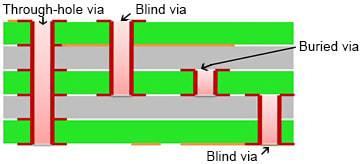
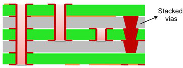
In PCB designing the term “via” is extensively used. It is actually the connection source in the form of copper-plated hole which connects different layers in the PCB. Different vias can be used but the most widely standard via used across the world in every PCB is the through-hole via. Several disadvantages are associated with through-hole via specifically in surface mount technological applications. Because of these disadvantages, through-hole vias are replaced by two additional vias such blind via and buried via. Both these vias (blind and buried) have processing in a variety of different measuring features which include plugged copper mask via, plugged solder mask via, plated via and staggered via. A simple comparison of through-hole via, blind via and buried via is depicted in Figure below.
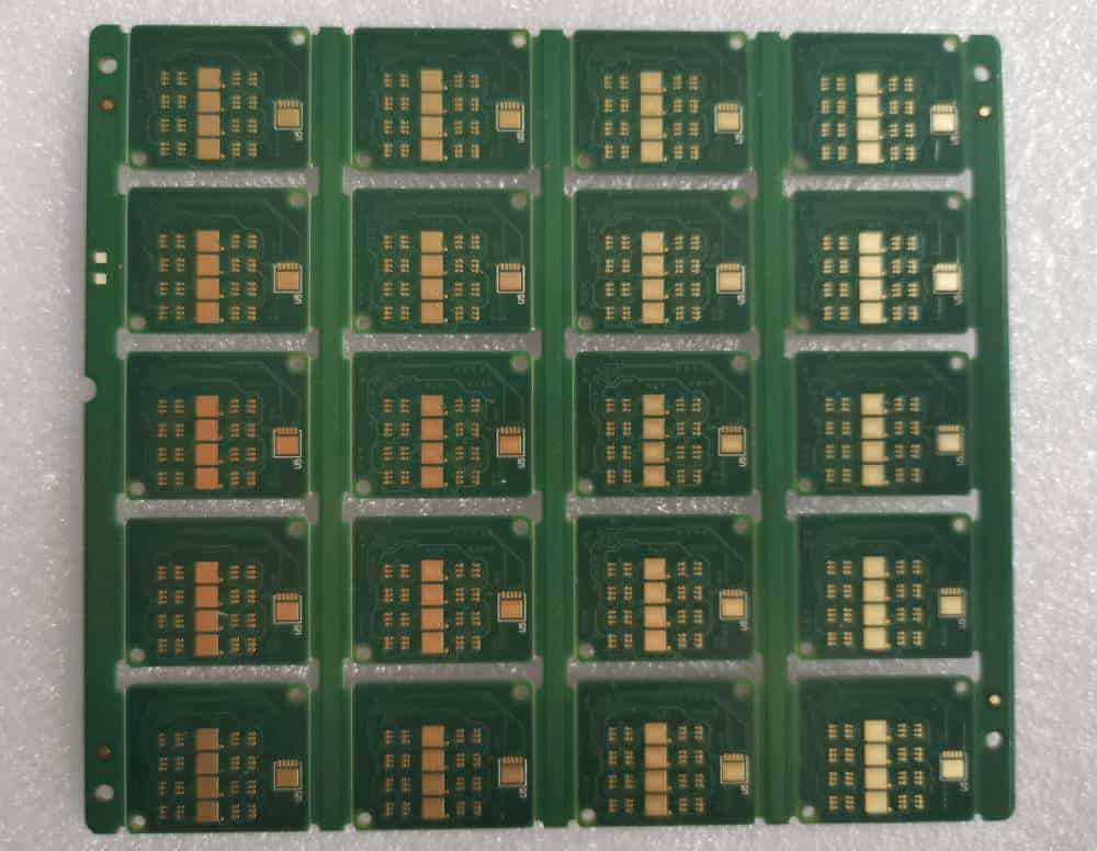
8Layer Blind & Buried PCB – 1-2 2-3 1-3 3-6 6-7 7-8 6-8.DRL 2 time laser drilling
Both blind and buried vias are used for connection of different PCB layers. What are the major differences in these types of vias are discussed in this section? The blind via provides an interconnection of the outer layer with a single or multiple inner PCB layers whereas only inner layers are interconnected in the buried via and the board is completely kept hidden and invisible from external environment of the PCB. Both these vias have great advantages in HDI PCB due to their optimal density deprived of increase in the size of board or requiring the number of layers in the PCB board.
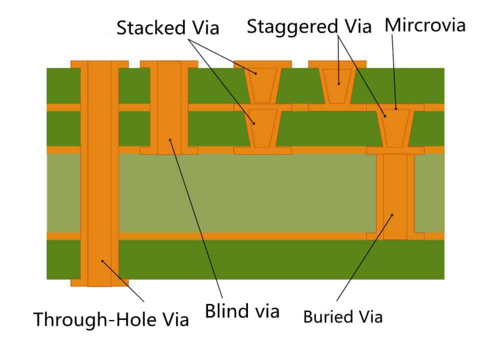
There is another classification of PCB board via and known as stacked via and micro via. These are discussed in the next section along with their pros and cons.
The stacked via is basically meant for improving further the size and density of PCBs during the process of their manufacturing. These two factors have great importance in todays’ modern miniaturizing and high transmitting signaling with requirements of speed in several applications and areas. If there is a consideration of blind via having a 1:1 or more aspect ratio or the process of drilling requires multiple layers to cover then the best way to get the interconnection among the layers can be stacked via. Additionally, the lamination of stacked via is either by blind or buried for building multiple layers within the circuit board to be built together around the same origin or central point whereas there is no lamination around the center in the staggered via.
Several advantages are associated with the stacked via such as providing greater space in the board by saving the area, enhances the overall density, better in terms of flexibility in terms of internal connection, capacity of better routing and minimum parasitic capacitance. Similarly, the most important and bigger disadvantage of PCB stacked via is their highest cost as compared to the standard through-hole via or blind and buried via that significantly reduces their use by common or student designers and favorite among the people working in bigger professional environments.
Similarly, there is another kind of via known as micro via which is comparatively smaller than other types of vias. This type of via is the favorite among PCB designers due to smaller diameter, greater space for routing on the PCB board and have lower parasitic capacitance in high-speed circuits and systems. Nevertheless, there are some disadvantages of micro via such as needing more time for drilling and off-center via moves. As per the rules ofpcba360 , the diameter of the micro via is kept as lower as 0.1 mm in PCB designing boards.
Contact pcba360 for PCBs with Blind/Buried Vias and Stacked Vias/Micro vias
pcba360 is one of the most leading PCB board designing manufacturing company that have several years of experience in designing the PCBs using both the blind and buried vias. This is the company which builds the PCB circuits based on the via types as per recommendation, desires and needs of the users for specific applications. In Table 1, the design parameters for PCB board by pcba360 using both the blind and buried vias are briefly explained and depicted along with the needs and applications.
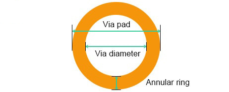
Figure 3 shows a difference between the most important design parameters provided by the pcba360 . These two important parameters are via type and via diameter. Figure 3 clear mentions via pad, via diameter and annular ring of a specific PCB layout design using the specific via based on its application.
The table below is illustrating different types of vias. The table is alos having information of the various dimensions necessary for the vias to be implemented in the printed circuit boards. Moreover, aspect ratio is also mentioned against each type of via.

pcba360 provides a continuously check and balance and information about the PCB design manufacturing using the particular via types. There is access to consumers for knowing the information their needs and interests to learn about the various via types. The users should get in touch for understanding the trends in via types for optimizing the value of desired PCB boards. The user can get access to the specific printed circuit just by clicking on the link given below.
In high-speed PCB design, via design is essential. This includes the hole, the pad area around the hole, and the power layer isolation area. There are three types: blind via, buried via, and through-hole. After analyzing the parasitic capacitance and inductance of vias, we have summarized some considerations in high-speed PCB via design.
Via is a crucial factor in multilayer PCB design. A via is mainly composed of three parts: the hole, the pad area around the hole, and the power layer’s isolation area. The process of the via is to plate a layer of metal by Chemical Vapor Deposition on the cylindrical surface of the hole wall, for connecting the copper foils in the middle layer. The upper and lower sides of the via are made into pad shapes, directly connected to the upper and lower sides of the circuit. Vias can be used for electrical connection, fixing or location devices.
There are three types of VIAS: blind holes, buried holes, and through–holes.
Blind holesare located at the top and bottom surfaces of PCB. For connections between surface and inner lines, the hole depth and diameter usually do not exceed a specific ratio.
Buried holesare connection holes in the inner layer of a PCB that does not extend to the surface of the circuit board.
Both blind vias and buried vias are located in the inner layer of the circuit board, which uses a through-hole forming process before lamination. There may be several inner layers overlapped during the process.
Through–holes pass through the whole circuit board and can be used for internal interconnection or as a component location hole. Because the through-hole is easy to use at a lower cost, we always use through-holes in PCB. The via shown as below:
The via itself has parasitic capacitance to ground. Assuming the diameter of the isolation hole on the ground layer is D2, the diameter of the via pad is D1, the thickness of the PCB is T, and the dielectric constant of substrate is ε, then the parasitic capacitance of the hole is approximately:
C =1.41ε TD1/(D2-D1)
The main effect of the parasitic capacitance of the via is to extend the rise time of the signal and reduce the speed of the circuit. The smaller the capacitance value, the smaller the effect.
Parasitic inductance exists in the via itself. In high-speed PCB design, the parasitic inductance of vias is more harmful than the influence of parasitic capacitance.
The parasitic series inductance through the hole will weaken the bypass capacitor’s function and the filtering effect of the whole power supply system. If the inductance of the via is L, the length is L, and the diameter is D, then the parasitic inductance of the hole is approximately:
L=5.08h[ln(4h/d)+1]
From the formula, the diameter of the via has a small influence on the inductance, while the length has the largest influence.
Non-through vias include blind vias and buried vias.In the non-through via technology, the application of blind and buried vias can greatly reduce the PCB size and layer count, improve electromagnetic compatibility, reduce costs, and cause the design work to be more efficient. In traditional PCB design and processing, through-holes can cause many problems. First, they occupy a lot of valuable space. Secondly, many through-holes in one place also be a huge obstacle to routing the inner layer of multilayer PCB. These through-holes take up the wiring space, and they intensively pass through the power supply and the ground layer. They can also destroy the impedance characteristics, making the power supply and ground layer ineffective. Additionally, mechanical drilling is 20 times as much work as non-through via technology.
In PCB design, although the size of pads and vias have gradually decreased, if the board thickness is not proportionally reduced, the aspect ratio of the via will increase, leading to a reduction in reliability. With the advancement in laser drilling technology and plasma dry etching technology, it is possible to make smaller blind and buried holes. If the diameter of these non-through vias is 0.3mm, the parasitic parameters will be about 1/10 of the original conventional holes, which improves the reliability of the PCB.
Due to the non-through via technology, there are fewer large through-holes and more spacing for PCB routing. The remaining space can be used for large area shielding to improve EMI/RFI performance. Simultaneously, more remaining space can also be used for the inner layer to partially shield the device and key network cables, which leads to an increase in electrical performance. The use of non-through vias makes it easier to fan out the component pins, making it easy to route high-density pin devices (such as BGA package devices), shortening the wiring length, and meeting the timing requirements of high-speed circuits.
In ordinary PCB design, the parasitic capacitance and parasitic inductance of the via have little effect on the PCB design.
For 1 to 4 layer PCB design, it is better to use 0.36mm/0.61mm/1.02mm (drilled hole/pad/power isolation area) via holes.
Some signal wires with special requirements, such as power wires, ground wires, clock wires, etc., can choose 0.41mm/0.81mm/1.32mm hole. They can also choose other sizes of holes according to the actual conditions.
From the above analysis of the parasitic characteristics of vias, in high-speed PCB design, simple vias often negatively affect circuit design. In order to reduce the adverse effects caused by the parasitic effects of the vias, we should note:
(1) Choose a reasonable hole size. For multilayer general-density PCB design, it is better to use 0.25mm/0.51mm/0.91mm (drilling/pad/power isolation area) vias.For some high-density PCBs, 0.20mm/0.46mm/0.86mm vias can also be used; non-through viasare also an option. For power or ground vias, consider using a larger size to reduce impedance.
(2) The larger the power isolation area, the better, considering the via density on the PCB, generally D1=D2+0.41.
(3) Try not to change the layers of the signal traces on the PCB, they are meant to reduce the hole quantity as much as possible.
(4) Using a thinner PCB helps reduce the two parasitic parameters of vias.
(5) The power and ground pins should be as close to the vias as possible. It is better to have shorter leads between the vias and the pins because they will increase inductance. At the same time, the power and ground lines should be as thick as possible to reduce impedance.
(6) Place some ground vias near the vias of the signal layer to provide a short-distance loop for the signal.
It is necessary to give concrete analyses of the problem. Considering both cost and signal quality, designers always want to make the holes as small as possible in high-speed PCB design, which leaves more wiring space. In addition, the smaller the via, the smaller its parasitic capacitance, which is more suitable for high-speed circuits.
In high-density PCB design, non-through vias and the reduction of vias size increase the cost. There is a limit to reducing via size, restricted by PCB manufacturer’s drilling and electroplating technology. These are the balance factors that need to be taken into consideration.
Since through-holes are easier to produce at a lower cost, most PCB designers like to use them. From a design point of view, a via is mainly composed of two parts, the drill hole in the middle and the pad area around the drill. The size of these two parts determines the size of the via. The designers always want to make the holes as small as possible in high-speed PCB design, which leaves more wiring space. In addition, the smaller the via, the smaller its parasitic capacitance, which is more suitable for high-speed circuits.
The use of non-through vias and the reduction of vias size increase the cost. There is a limit to reducing via size, restricted by PCB manufacturer’s drilling and electroplating technology. The smaller the hole, the longer it takes to drill and the easier it is to deviate from the center position. When the depth of the hole is more than six times the hole’s diameter, it is impossible to guarantee the uniform copper plating of the hole wall. For example, if the thickness (through-hole depth) of a standard 6-layer PCB board is 50Mil, then under normal conditions, the minimum drilling diameter provided by the PCB manufacturer can only reach 8Mil.
With the development of laser drilling technology, the size of the hole can be smaller. Generally, a via with a diameter 6Mils or less is called a microhole. Microvias are often used in HDI (High-Density Interconnect Structure) design.
Micro via technology allows vias to be directly drilled on the pad (via-in-pad), which dramatically improves circuit performance and saves wiring space.
The through-hole in the transmission line is the discontinuous impedance breakpoint, which will cause signal reflection.
Generally, the equivalent impedance of a via is about 12% lower than that of a transmission line. For example, the impedance of a 50 ohms transmission line will decrease by 6 ohms when passing through a via.
However, the reflection caused by the discontinuous impedance of the via is negligible, and its reflection coefficient is only: (44-50)/(44+50)=-0.06. The problems caused by vias are more concentrated on the influence of parasitic capacitance and inductance.
Buried via
The use of blind holes and buried holes is an effective method to increase the density of multilayer boards, reduce the number of layers and board size, and significantly reduce the number of plated through-holes. Almost all BUM boards use buried and blind via structures. Buried holes and blind holes are mostly small holes with a diameter of 0.05 to 0.15 mm. Buried holes are manufactured on the inner thin laminate using the same process of manufacturing double-sided PCBs. In contrast, the manufacturing of blind holes started with a small hole CNC bed that controls the Z-axis depth, laser drilling, plasma etching, and photo-induced holes are now commonly used. Laser drilling has carbon dioxide laser machine and Nd: YAG ultraviolet laser machine. The carbon dioxide laser drilling machine of Hitachi, Japan, has a laser wavelength of 9.4 Hongm, and one blind hole is drilled three times, which can drill 30,000 holes per minute. With the development of electronic products that require high density and high precision, the same requirements are put forward on circuit boards accordingly. The most effective way to increase the PCB density is to reduce the number of through-holes and accurately set blind holes and buried holes.
The process of designing and making buried holes is more complicated and more costly than traditional multilayer boards. The figure shows the difference between the traditional inner layer and the inner layer with buried holes.
Figure 20.3 explains the stack-up of 8 layer PCB with buried-hole.

The double-sided SMD design of the board will have the top layer and bottom layer. The I/O vias will interfere with each other, but when there is a VIP (Via-in-pad) design, it will have more trouble. Blind holes can solve this problem. In addition to the prevalence of radio communication, circuit design must reach the RF (Radiofrequency) range, over 1GHz. Blind hole design can meet this requirement. Figure 20.5 is the general specification of blind holes.

There are three different methods to make the blind hole PCB:
In the traditional multilayer board manufacturing process, the drilling machine is used to set the Z-axis depth for drilling, but there are some concerns:
a.Only one piece can be drilled at a time, and the output is very low.
b.The drilling machine table must be level, and the drilling depth of each spindle must be the same. Otherwise, it is difficult to control the depth of each hole.
c.Electroplating in the hole is difficult, especially if the depth is greater than the hole diameter, it is almost impossible to electroplate in the hole.
Due to the limitations of the processes mentioned above, this method is becoming less popular.
Take an 8-layer PCB board as an example (see Figure 20.6)

The Sequential lamination can make blind and buried holes at the same time. First, make the circuit and PTH of the four inner layers (six layers + double layer, top and double bottom layer, and inner four layers). Then laminate the four pieces together into a four-layer board, then make a through-hole. This method has a long process and a higher cost, so it is not universal.
This method is the most popular in the industry, and many domestic manufacturers have similar manufacturing experience.
This method extends the above-mentioned sequential lamination concept, adding layer by layer to the outside of the board and using non-machine-drilled blind holes as the interconnection between the layers. Here are the three main methods:
In addition to the comparison in Table 20.1, the above three commonly used build-up methods are shown in Figure 20.7.

The three blind hole manufacturing processes should be transparent. Chemical Etching is not introduced here. Figure 20.8 shows a three-dimensional diagram of various hole forming methods for reference.

The most effective way to increase PCB density is to reduce the number of through-holes and accurately set blind and buried holes.
A: Through-holes refer to holes drilled through each layer, and blind holes are non-drilled through holes. ( Eight-layer board example: through-hole, blind hole, buried hole)
B: Blind hole subdivision: (blind hole, buried hole ( it is not visible from outer layer)).
C: The different production processes – Blind holes are drilled before lamination, while through-holes are drilled after lamination.
2. Manufacturing Method
A: Drill belt
Note that when the laser hole is sleeved with the inner buried hole, the holes of the two drill belts are in the same position. You need to ask the customer to move the laser hole position to ensure the electrical connection.
B:Production panel board edge process hole: ordinary multilayer board: no drilling in the inner layer.
Blind Hole Board
All tooling holes are drilled, Note Rivets gh; need to be punched to avoid misalignment(aoigh also the same),The panel board edge needs to be drilled to distinguish each board.
3. Film Modify:
( 1 ) Indicate that the film produces positive and negative films.
General principle: If the board thickness is greater than 8mil (without copper), use the positive film process. If the board thickness is less than 8mil (without copper), use the negative film process (thin board).
When the line width and line gap are large, the copper thickness at d/f should be considered, not the bottom copper thickness. The blind hole ring can be made 5mil; it is not necessary to make 7mil.
The inner independent pad corresponding to the blind hole needs to be retained. Holes cannot be made without ring holes.
4.Process:
The process of buried-hole PCB is the same as the standard double-sided board.
Blind Hole PCB, one side hole is visible on the outer layer.
Positive film process: Single-sided d/f must be made, and it cannot be misaligned (when the double-sided bottom copper is inconsistent). When d/f is exposed, the glossy copper surface is covered with black tape to prevent light transmission.
The blind hole board needs to be patterned more than twice. The finished product can be easily made to be too thick. Therefore, please pay attention to the board thickness and copper thickness, and indicate the range after etching.
After lamination, use the x-ray machine to punch out the target holes for the multilayer board.
Negative film process: For thin boards (<12mil with copper), they cannot be produced in the pattern plated line.
They must be produced in the immersion gold process. However, one side cannot draw current, making it impossible to do a single side with no current or small current. If the positive film process is adopted, the copper thickness on one side is too thick, which causes etching difficulties and the phenomenon of thin lines. Therefore, such boards use the negative film process.
5. The drilling sequence of through holes and blind holes is different.
Blind hole board is easy to deform. It is difficult to control the multilayer board’s alignment and the distance between tubes when cut lamination. Therefore, we only cut horizontal or straight lamination.
This kind of board should pay attention to the use of resin plug hole before making the circuit not to cause greater damage to the circuit.
Blind and Buried vias

Features of blind buried vias

Board technological process 2:
Cutting (2/3 layer) – drilling LDI hole – inner layer pattern – inner layer etching – inner layer AOI – browning – lamination ( lamination RCC 1/3 layer) – drilling – laser drilling – normal process.
Schematic diagram of 2+2 blind hole board:

Board technological process 3
Cutting – drilling blind hole – deburring – electroless copper – plate plating – inner layer plating hole film – electroplating hole – inner layer pattern – inner layer etching – inner layer AOI – browning, laminating – de-gluing, drilling – normal process
Schematic diagram of 4-layer HDI blind buried board:

Board technological process 4
Cutting (2/3 layer) – drilling LDI hole – inner layer pattern – inner layer etching – inner layer AOI – browning, laminating (lamination RCC layer) – drilling – laser drilling – normal process.
Schematic diagram of 6-layer HDI blind buried board

Board technological process 5
Cutting (3/4 layer) – drilling LDI hole – inner layer pattern – inner layer etching – inner layer AOI – browning – lamination (laminating to 2/5 layer) – drilling (drilling 2/5 layer buried hole) – electroless copper – plate plating – inner layer plated film – electroplated hole – inner layer pattern – inner layer etching – inner layer AOI – browning, lamination (press RCC layer) – drilling – laser drilling – normal process (If there is no buried hole in the 2/5 layer – the board will turn to the inner layer pattern after drilling the LDI hole).
Schematic diagram of 6-layer blind buried vias board:

Board technological process 6
Cutting, drilling mechanical blind buried holes, deburring, electroless copper, plate plating, inner layer plated film, electroplated hole, inner layer pattern, inner layer etching, inner layer AOI, browning, lamination, degumming, drilling Hole, normal process (for example, if there are no buried holes on 3/4 layer, the inner layer core board is transferred to the inner layer pattern after drilling the LDI hole).
Schematic diagram of 3+3 (RCC) blind buried vias board:

Board technological process 7
Schematic diagram of 4+2 blind buried vias board:

Board technological process 8
Schematic diagram of 4+4 blind buried vias board:

Board technological process9
Cutting (2/3, 6/7 layers), drilling LDI holes, inner layer pattern, inner layer etching, inner layer AOI, browning, lamination (laminating to 1/4, 5/8 layers), drilling ( Drill 1/4, 5/8 layer blind holes), electroless copper, plate plating, inner layer plated film, electroplated holes, inner layer pattern, inner layer etching, inner layer AOI, browning, lamination (laminating 1/ 8 layers), glue removal, drilling, normal process (If there are no blind holes on 1/4 or 5/8 layers, the board will be transferred to the inner layer pattern after drilling the LDI holes).
8 layer 2 Step HDI blind and buried PCB

Board technological process 10
Cut Material (3/4、5/6 Layer )、Drilling LDI Hole、inner layer pattern、Inner Layer Etching、Inner Layer AOI、Brown Oxidation、laminate(Press 2/7 layer)、Drilling (Drill 2/7 layer buried hole)、Electroless Copper、Plating Surface Copper 、Inner hole Plating fIim、Hole Plating、inner layer pattern、Inner etching、Inner AOI、Brown Oxidation、Laminate(Press RCC layer)、Drilling 、Laser Drilling (1-2、1-3、7-8、6-8)、Normal Process(If 2/7 layer no buried hOLE,After drill LDI hole then switch to inner layer pattern)
Schematic diagram of 8-layer 2-level HDI blind buried vias board:

Board technological process 11
Cutting (4/5 layer) – drilling LDI hole – inner layer pattern – inner layer etching – inner layer AOI – browning, lamination (laminating to 3/6 layer), drilling (drilling 2/6 layer buried hole) – electroless copper, plate plating – inner layer plated hole film – electroplated hole – inner layer pattern – inner layer etching – inner layer AOI – browning, lamination (press RCC 2/7 layer) – drilling – laser drilling, electroless copper – plate plating – inner layer plated film – electroplated hole – inner layer pattern – inner layer etching – inner layer AOI – browning – lamination (laminating RCC 1/8 layer) – drilling, laser drilling – normal Process (If there are no buried holes on 3/6 layer – the board will be transferred to the inner layer pattern after drilling the LDI hole).
C4 Jinxiongdakejiyuan Huanguannan rd, Guanhushequ, Longhua district Shenzhen China
 sales@pcba360.com
 PCBA360
 +86-755-84717796
Certifications

Delivery


<

 Quote
Quote