


PCBA processing technology has become increasingly mature and has a wide range of applications. It plays a key role in today’s various intelligent devices.To make the board understand the function of the expected design and the hardware, it needs the matching support of software and program.
Here is list of different components programming :
1.fpga programming:xilinx fpga programming,python fpga programming,altera fpga programming
2.pic programming or pic microcontroller: programming,pic16f877a programming,pic12f675 programming,microchip pic programmer,pic controller programming,pic16f84a programming,pic32 programming,pic12f508 programming
How to transfer Program Into Chip?
I believe you have already known that the answer is “programming”, someone also called “burning”.Programming, the process of transferring the program into the chip’s internal storage space.There are offline programming and online programming.
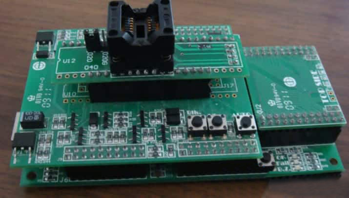
1.Offline programming
Offline programming is compatible with chips in different packages by the different adapters. The chip can be used with the adapter to achieve program burning.
The adapter is a precision fixture. The different chips and packages need different adapters.
Nowadays, the package is developing in small and flat BGA, QFN, etc., such as the widely used Emmc chips. At the same time, the price of those adapters is not low.

If there is an error in the production pcba test, you need to remove the chip from the adapter and re-program according to the prescribed process, which will waste time, energy and add additional costs.
There are some emergencies in PCBA production. If the temperature resistance of the circuit board is not sufficient, the chip will be deformed when you remove the chips, which will increase the risk of scrapping.

2.Online programming
The online programming uses the chip’s standard communication bus, such as USB, SWD, JTAG, UART, etc. The interface is generally fixed, and there are fewer pins to be connected during programming.
Since the interface communication rate is not high, general cables can be used for burning without high consumption.
Because the online burning is programmed by wire connection, if an error is found during the production test, the faulty PCBA can be traced back and re-burned without disassembling the chip. This not only saves production costs but also increases the efficiency of programming.
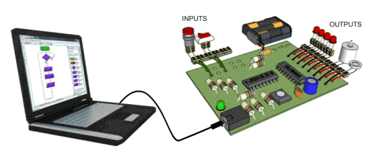
More importantly, the production line is developing towards automation. More and more manufacturers are adding functional test machines such as ICT and FCT to the production line. The production method, using automatic fixtures and online burning, can be omitted in the burning stage.
In the manual operation, the board is attached after it’s directly burned, and then the PCBA is sent to the test machine for testing. The entire production process is fully automated, which can significantly improve production efficiency.
Therefore, in PCBA processing, the advantages of online burning are significant. It is becoming one of the industry’s important indicators to measure PCBA manufacturers’ process precision, production efficiency, cost, quality control, scale, and capital.
Universal IC Programming Tutorial
All IC chips from the buyer are blank. We program the latest version of the software before SMT work. This is an important and necessary step for the chip test; usually, the work will be done by an SMT supplier like XDF.
IC Programming Explanation
OTP:One Times Program
FLASH Chip: A chip can be flashed and re-programmed many times
MASK: The Chips MCU already has the software inside. It can’t be programmed any further.
Programming chip:Programming the software into blank chips; all flash chips are programming chip
IC Chip Programming Steps and Method
1ST :The tools should be prepare before programming
Wired electrostatic ring
Pen
Computer
Programmer(GAME8 and ALL-11)
Second: The IC chip programming tips
Be careful when placing the IC to avoiddamaging the IC and programming socket.
Place IC chip correctly. The disassembled IC must be checked whether tin short circuit on the pins first, otherwise the programming socket will be easily damaged.
The workers must be trained before programming and must not use other software on the computer.
If a faultis found, please report to a manager to solve the problem at once.
Third: IC chip programming steps and method
Connect the programmer cable first,install the corresponding IC socket into the writer socket, and turn on the computer and the programmer.
Run the programming software: Double-click the “GANG-08″with the mouse (different programming sockets correspond to different burning software).
Choose the IC brand. After the program startup screen appears, click the “Device”menu to call up the IC brand selection table. Then select the brand corresponding to the IC to be burned, and then click “OK”.
Select the IC Part No: The IC Part No produced by the company, click “Run”after selecting the IC Part No l. If you want to select a jumper for the programming socket at this time, follow the computer’s prompt to jumper and jumper the line, Then click “OK”. If there is no jumper on the programming socket, it will enter the programming interface directly.
Load the software to be burned: Click the menu “File”, select “Load File To Programmer Buffer”, then select the software click “Open”, then select “00”, and click OK.
Check the software checksum (Buffer Checksum): After the software is loaded, a four-digit checksum will appear after the Buffer Checksum. This code should correspond to the “Electronic Design Document Notice” checksumto indicate the need to burn The recorded software is correct. If it is incorrect, it should be reported to the relevant department immediately for resolution.
Programming software: Click the “Program”button to load the IC into the IC socket, and then press the burning button on the burning socket. An “OK” will be displayed if the programming is successful, and the red “Error” will be displayed if the programming fails. The OK indicator light of each programming socket corresponds to the IC with the program. If it is on, it indicates that the IC programming is successful.
Make a mark, put a sticker on the IC that burned OK. If the burn failed,put it on another socket and program it again. Put it in the defective box if the IC is damaged, and make a mark.
Fourth: failed IC chip programming steps
Repeat steps1 to 6.
After the programming interface appears, click the “Auto”buttonand select the three options “Erase, Program, Verify”.
Place the IC to the socket, and then press the burning button on the socket. “OK” will be displayed if the burning is successful, and the red “Error” will be displayed if the burning fails. The OK indicator light of each programming socket corresponding to the IC with the program. If it is on, it indicates that the IC programming is successful.
Puta sticker on the IC that burned OK. If the burn fails again or it is determined that the IC is damaged, return it to the warehouse.
Fifth: IC programming verification steps
Place the IC that should be programmed in to socket. Burn the IC according to the work instruction and marked it.
After the programming is successful, put the IC into other sockets with different numbers, then select “VERIFY”in the menu, and press “RUN”to start the verification. If all appears “OK”, then put the IC into other programming sockets and check If the check is OK, it means that the programming socket is OK.
If “VERIFY”fails, first install anotherIC that was previously verified as OK into the failed IC socket. If the same socket still fails the test, it means that the socket may be damaged. If there is an error in programming the IC data, re-insert the IC into an undamaged If it is confirmed to be damaged, immediately stop programming in this socket. Immediately report the situation to the relevant personnel and recheck the burned IC.
IC Programming Service
First: IC burning project
IC types:MCU/MPU, EPROM, EEPROM, FLASH, Nand Flash, PLD/CPLD, SD Card, TF Card, CF Card, eMMC Card, eMMC, MoviNand, OneNand.
IC footprint DIP/SDIP/SOP/MSOP/QSOP/SSOP/TSOP/TSSOP/PLCC/QFP/QFN/MLP/MLF/BGA/CSP/SOT/DFN…
IC package:Tray, tube, tape
Nand Flash: SAMSUNG(K9F1G08),TOSHIBA(TC58NVG0S3),HYNIX(HY27)…
IC manufacturer:USA, Japan, Taiwan, European brands
Second: Support large-volume, multi-variety IC burning service
Third eMMC programming solution
eMMC is a standard specification for embedded memory established by the Multimedia Card Association. It is mainly for mobile phone products and simplifies the design of memory. It uses multi-chip packaging (MCP) to package NAND Flash chips and control chips into one chip. eMMC has multi-function, including storage and boot function that replaces NOR Flash.
The biggest advantage is that mobile phone manufacturers do not need to redesign specifications due to NAND Flash vendors or different process generations, and need to deal with NAND Flash compatibility and management issues. Mobile phone customers only need to purchase eMMC chips and put them in mobile phones, which not only shortens the time-to-market and R&D costs of new products, but also accelerates the product launch.
PRO-808 eMMC/SD duplicator has high performance, PC-free independent operation. It also has a single female port and 8 target slots, supports MMC version 4.3/4.4/4.41 protocol, and compatible with eMMC/MMC/RS-MMC cards. eMMC is currently on the market. All mainstream brands support copying. Five operation modes are provided: Partition,
Auto, Mirror, File and User mode copy and verification operations, suitable for various application copy programs. It also supports the eMMC general partition table/user-defined enhanced area (Partition/Enhanced User Area) copy and verification operations. The burning speed is up to 22MB/s, and the checksum value is generated during the verification process. It also provides RS232 interface x2, connect to PC to remote multi-machine control, up to 8 PRO-808 can be connected in series.
More detailed product features and specifications:
SD List
SDCPM‐I1 VER.02.01.48
SANDISK ‐ ‐ SD microSD 1
SANDISK 4 ‐ SDXC SD 64
TOSHIBA 4 ‐ SDHC SD 8
KINGSTON 4 SD4 SDHC SD 4
TRANSCEND 6 ‐ SDHC SD 4
APACER 60x ‐ SD SD 2
SILICONPOWER 45x ‐ SD SD 2
ATP 6 ‐ SDHC SD 4
KINGSTON 4 SDC/4GB SDHC microSD 4
KINGSTON ‐ SDC/2GB SD microSD 2
eMMC IC List
SDCPM‐I1 VER.02.01.55
VENDOR PART NUMBER MMC VER PACKAGE
CAPACITY
(GB)
KINGSTON KE44B‐25AN/2GB 4.41 BA 2
KINGSTON KE44A‐26BN/4GB 4.4 AA 4
HYNIX H26M21001ECR 4.41 BA 2
HYNIX H9TP33A8LDMCMR‐KYM 4.41 POP 4
HYNIX H9TU33A6ADMCLR 4.41 POP 4
PHISON PSW4A11‐2G 4.41 AA 2
SAMSUNG KLM4G2DEJE 4.41 AA 4
SAMSUNG KLMAG4FEJA‐A001 4.41 AA 16
SAMSUNG KLMBG8FEJA‐A001 4.41 AA 32
SANDISK SDIN4C1‐4G* 4.3 AA 4
SANDISK SDIN4C1‐8G* 4.3 AA 8
SANDISK SDIN4C2‐2G 4.3+ AA 2
SANDISK SDIN4C2‐4G 4.3+ AA 4
SANDISK SDIN4C2‐8G 4.3+ AA 8
SANDISK SDIN4C2‐16G 4.3+ AA 16
SANDISK SDIN5B2‐32G 4.41 AA 32
SANDISK SDIN5C2‐2G 4.41 BA 2
SANDISK SDIN5C2‐4G 4.41 AA 4
SANDISK SDIN5C2‐8G 4.41 AA 8
SANDISK SDIN5C2‐16G 4.41 AA 16
SANDISK SDIN5D2‐2G 4.41 BA 2
TOSHIBA THGBM2G6D2FBAI9 4.4 AA 8
TOSHIBA THGBM2G7D4FBAI9 4.4 AA 16
TOSHIBA THGBM2G8D8FBAIB 4.4 AA 32
TOSHIBA THGBM3G4D1FBAIG 4.41 BA 2
TOSHIBA THGBM3G5D1FBAIE 4.41 AA 4
PKG. CODE PKG. DETAIL
AA 169 ball, 12x16x1.4mm
AB 169 ball, 12x18x1.4mm
AC 169 ball, 14x18x1.4mm
BA 153 ball, 11.5x13x1.3mm
superpro 610p
soic8 sop8
xeltek superpro 610p
ic 24c08
xeltek superpro 6100
ic 24c16
xeltek superpro 6100n
memory ic 24c08
sop8 chip
ch341a ic
xeltek 6100
ic ch341a
xeltek 6100n
mlx90316 programming
sn8p2501bpb programming
SD copy device, one copy twelve
Designed for SAS interface hard drives used in the latest server-grade computers. Compatible with a variety of hard drives, including SAS/SATA (2.5″ and 3.5″), SSD solid-state drives (SAS/SATA interface). IDE and ZIF interface hard disks can also be copied through the optional adapter board.
High-speed performance bandwidth design is up to 18GB per minute, up to 120MB per second measured copy speed. The access and copy speed of the hard disk’s inner and outer rings are also different. This is currently the fastest SAS, and the SATA interface copy platform is sufficient for fast copying needs in the next few years.
Simplified design and modular structure
Powerful and versatile
Innovative copy capability of RAID disk arrays
Safe power environment
Fourth Nand programming solution
Talking about a few key points of NAND programming, why does programming NAND Flash often fail? Why does the system not work after some NAND chips are mounted on the board? After asking so many why, I will ask a question: Do you understand NAND Flash’s characteristics and its programming key points?
1. NANDFlashSpec
1) Bit flip
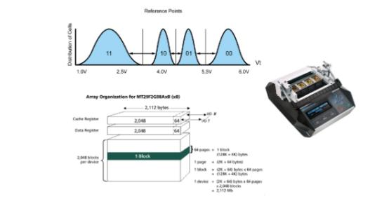
In NAND flash memory, data storage is completed by charging the storage cell (Cell), and the threshold voltage of the storage cell corresponds to the data value. When reading, the data value is obtained by comparing its threshold voltage with the reference point. For SLC, there are only two states and one reference point. For 2-Bits MLC, it has four states and three reference points. TLC has more status and reference points.
When the read data value does not match the threshold voltage corresponding to the data value during programming, it indicates that the data has bit flipped, which brings reliability problems. The most common cause of bit flips is threshold voltage drift caused by “program disturb.”
2) Storage structure
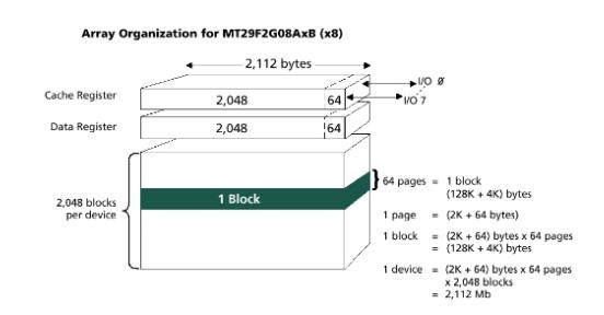
NAND Flash memory is composed of multiple blocks, and each block is composed of multiple pages. The size of pages is generally 512+16Bytes, 2K+64Bytes, and 4096+128Bytes. Page is the basic unit of reading and programming, and the basic unit of the erasing unit is block.
The page of NAND Flash contains two fields: Main Area and Spare Area. The “Main Area” is also often called the data area. The spare area is a reserved area and is generally used to mark bad blocks and store the value of ECC. Some file systems use spare areas to record the number of erasures, file organization data, etc.
Bad block and ECC
The occurrence of bit flipping is random, and the number of bit errors will increase as the number of erasing and writing increases. But as long as the number of bit errors is within the range that ECC can correct, data integrity is always guaranteed. At some points, the bit error of each page may be very close to the limit that ECC can correct. The NAND control system must strictly prevent the bit error from exceeding the correctable range. Otherwise, data may be lost, or the system may not work normally. Therefore, these blocks must be marked as bad blocks.
Bad blocks should never be used to store data again. Because the generation of bad blocks is inevitable, NAND manufacturers will choose to mark certain blocks as bad blocks when testing the die rather than abandon the entire die. Therefore, most NANDs are already marked as bad when they leave the factory. Block of blocks. If a NAND block is marked as a bad block, then the NAND’s capacity is permanently reduced.
2.The key points of And system die mass production and burning
Due to the NAND Flash chip characteristics, they must be processed appropriately when using it as a storage medium so that the system can operate normally. The system sets the storage layout of each partition data in the NAND chip and performs bit error correction and bad block management on the Nand at the storage drive layer. This information needs to be clarified by the system/drive engineer.
In the R&D stage or small batch production stage, the method of programming is often used. The principle is to download the boot to the memory through the serial port and run, and then the boot will burn the kernel image, file system image, and other data from the SD card or network to the NAND Flash chip.
In order to improve production efficiency or other considerations, a writer will be used to mass-produce NAND Flash dies. Since the writer manufacturer does not know how the storage driver layer handles various characteristics of NAND, it is unreliable. If the programming is performed after configuration, the following situations often occur:
1. The programming fails, often because of the verification failures.
2. The programming passes, but the system cannot run after some chips are mounted on the board, or some modules appear when running with errors and exceptions. Most of these are not the burner’s problem, but that several important key points are not handled correctly when the NAND system is burned on the bare chip. Another reason might be the processing is not consistent with the target system. These key points include:
Bad boards solution
2) Partition
3) Error Correction Codes,ECC
Other factors affect the burning, such as spare area usage, unused fast formatting, dynamic metadata, etc. Still, we will only discuss the above few more common factors here.
Bad boards solution
Bad boards are generally identified according to the bad block mark position of the chip, and the bad boards processing strategy defines how the algorithm should deal with bad blocks. The strategy algorithm is responsible for writing the content that should have been written in the bad block to other optional good blocks. The most commonly used bad block processing strategy is to skip bad blocks. Other typical bad block skips with BBT and reserved block areas.
The processing strategy of skipping the bad board is the most basic and most commonly used bad block replacement strategy. When a bad block is encountered during programming, the algorithm skips the bad block and writes the data to the next good block. It will cause the location of physical data and logical data to shift, which usually requires partitioning to solve this problem.
(2) Partition
The NAND system, which adopts the processing strategy of skipping bad blocks, often divides the storage into several different physical areas. This is what we call the partition, which is conceptually similar to the partition of a computer hard disk.
Using partitions gives you the ability to ensure that your data can be stored in a pre-specified physical block area, even if some bad blocks are found before that. This helps low-level software components such as bootloaders and certain file system drivers that must be easily located.
When the replacement strategy of skipping bad blocks is used, the bad blocks will cause the data to move to the next good block. If the partition is set, you can instruct the writer to determine the boundary of the data to ensure that the data file will not encroach on the adjacent partition.
Figure 2.2.1 is the partition situation of a typical embedded Linux system.

(3) Error Correction Codes,ECC
It is necessary to adopt appropriate ECC algorithms for NAND storage systems of different processes and capacities. It is even necessary to ensure the reliability of the system. ECC error correction codes are generally stored in the spare area and are calculated from the data of a whole page or divided into several sections. Before data programming, ECC (except hardware ECC) needs to be prepared. If it is pure data, it needs to use the ECC algorithm to generate.
In mass production of NAND bare chips, it is important to know the error correction capability (error correction bits) of the ECC algorithm. To ensure production efficiency, it is impractical for the programmer to use ECC to verify the data. Through simple Data comparison, it can know the number of bit flips of the data. If the range of the number of flips is within the error correction range of the ECC algorithm, it is considered that the check should pass.
3 Customized Programming
For the above key points, if the writer software does not support the corresponding program, you need to contact the original factory to customize the relevant algorithm, such as bad block processing program, ECC program, etc.
Sixth MCU programming solution
MCU type can burn IC. Many single-chip controllers (SINGLE MCU) on the market can be used to burn one or more data through the matching burner. Usually, the MCU that can be programmed only once is called OTPMCU (English: ONE TIME PROGRAMMABLE MCU). In contrast to MTP, MCU (English is MULTI TIME PROGRAMMABLE MCU) is an MCU that can be programmed multiple times.
OTP MCUs are usually burned in by the manufacturer at one time through the matching burner before the product is assembled. Once this type of IC is burned, the burned data cannot be changed again.
MTP MCU is different from OTP MCU. This type of IC can be programmed and erased multiple times through the matching programmer. Some of the built-in FLASH MCUs can even be programmed not less than 100,000 times.
Programming room environment
Chips are electrostatic-sensitive components, so anti-static measures must be taken
(1)The electrostatic grounding wire of the chip room should be connected to the ground, not directly connected to the grounding wire of the power supply. The ground resistance of the electrostatic grounding system should be less than 0.5 ohm.
(2)Employees in the chip room should wear static wristbands and anti-static clothes when programming chips, and anti-static table mats should be laid on the work surface.
(3)The staff in the chip room must use the static ring tester to measure whether the static ring is good and the wearing specifications before officially burning the chip every day. It can not officially put into production until everything is normal.
(4)The OTP room has an anti-static grade of A, and the absolute value of static should be less than 100V.
Humidity greatly influencesstatic electricity, so a humidity tester should be added to the chip room for control. The best humidity range should be 50%-60%. If the humidity is low, you can use a humidifier or touch the ground. Sprinkle water to control the humidity within a proper range.
Best IC Chip Programmer and Tutorial
1. Renesas chip M37544, M37546, M38503 program burning:
First. “M37544G2A(SP)@SDIP32“ Select the chip model in the programming software. Connect to the Sirte 9000U programmer, open the software “SUPERPRO 9000U“, click “select device“, select “RENESAS” for the manufacturer name, select “M37544: “M37544G2A(SP)@ SDIP32“
M37546: “M37546G4(SP)@SDIP32“
M38503: “M38503G4A(SP)@SDIP42””,click “confirm” ;
Second. Start loading the program, click “Load File“, select the target file, click “Open“, then “Confirm“, load the sample into the writer. Click “Verify” to verify, and click “Edit Auto Burn“ displays shown in the box. Select “program“ and click “Add“; select “verify“ and click “Add“. The automatic burning method will add “program“ and “verify“. Click “Options” to pop up a drop-down dialog box, select “Mass Production Mode“; click “Auto” to start automatic programming. After programming is complete, replace the chip, and then cycle programming.

2. Renesas M38D24 program burning :
1)、Before working, connect the writer head to the writer and insert the USB plug on the Sirte 3000U writer into the USB port on the computer host, and the power indicator on the writer will be on.
2)、 Double-click the “SUPERPRO USB series” shortcut icon on the computer monitor to enter the main programming interface. Click “Select Device“, select “RENESAS” for the manufacturer name, select “M38D24G4FP@TQFP64” for the device name, and click “OK“.
3)、 Start loading the program, click “Load File“, select the target file, click “Open“, and then “Confirm“. Load the sample into the writer, click “Verify” to verify. After the verification is correct,click “Edit Auto Burn” to display the dialog box shown in the box.Select “program” and click “Add“. select “verify” and click “Add“. The automatic burning method will add “program” and “verify“. Click “Options” to pop up a drop-down dialog box, select “Mass Production Mode“; click “Auto” to start automatic programming. After programming is complete, replace the chip, click “Auto” again to program, and then cycle programming.
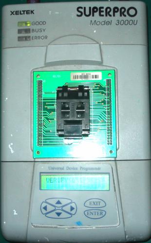
3. PIC18F45J10, dsPIC30F201, PIC18F45K20Program burning:
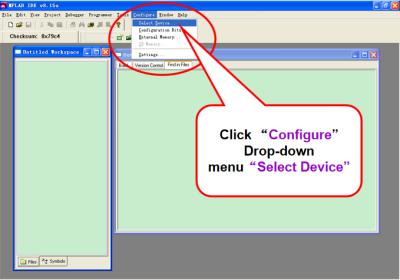
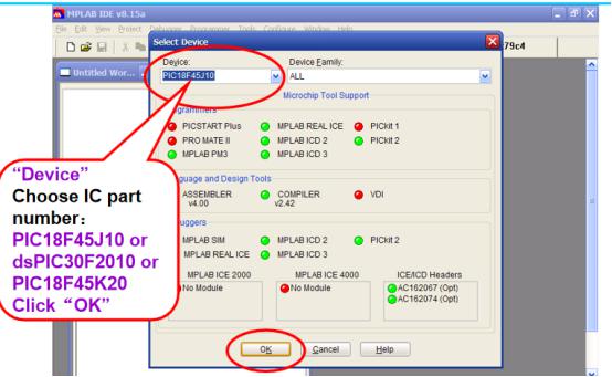
1)、Before proceeding with any work, first select the corresponding programming head according to the type of chip to be burned and place it on the bottom board of the writer (MPLAB PM3). Connect the power of the writer, then turn on the power and open the software “MPLAB IDE v8.5a“. Select the corresponding chip model, click “Configure” drop-down menu, and select “Select Device“. Select the corresponding chip model in the device item: PIC18F45J10 or dsPIC30F2010 or PIC18F45K20 and click “OK“.
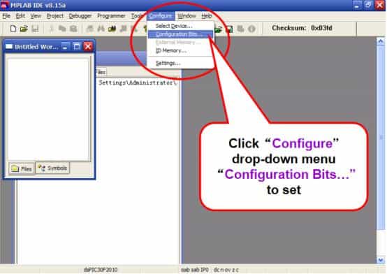
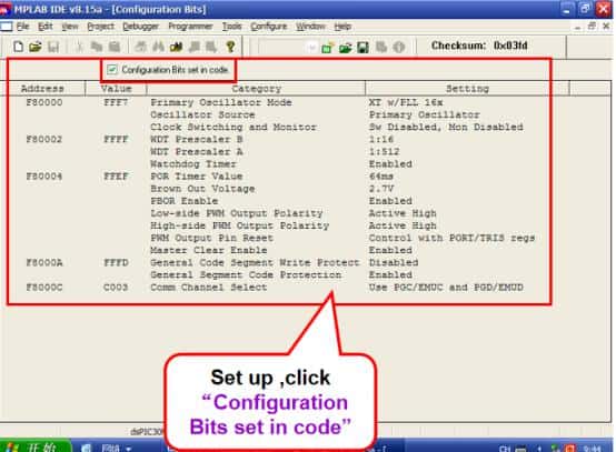
2)、Load program: Click “File” on the main menu, select “Import…” from the drop-down menu, select the target file, and click “Open“. Click “Configure” on the main menu and select “Configuration Bits…” in the drop-down menu to configure. When configuring, click “Configuration Bits set in code” to remove the configuration protection, click “OK“, and then start the configuration. After the configuration is complete, click “Configuration Bits set in code” to lock the configuration word.
3)、Click “Programmer” on the main menu, select the drop-down menu.
“Select Programmer” click “7. MPLAB PM3” in the menu.
Then click “Programmer” on the main menu, select the drop-down menu
“Enable Programmer“.
4)、Click the “Program” shortcut in the main menu to start programming. After it’s successful, replace the chip and click the “ENTER” button on the programmer to start offline programming.

Introduce step by step of MPLAB IDE v8.5a IC Programmer software
Click open MPLAB IDE v8.5a IC pr


C4 Jinxiongdakejiyuan Huanguannan rd, Guanhushequ, Longhua district Shenzhen China
 sales@pcba360.com
 PCBA360
 +86-755-84717796
Certifications

Delivery


<

 Quote
Quote