XDF provide impedance control PCB manufacturing, We accept multi-impedance control design, exactly manufacturing control with strip sample and impedance test report, Send your PCB files to Sales@pcba360.com, Estimate Cost Now !
Impedance Control PCB is the characteristic impedance of a transmission line formed by PCB conductors. It is relevant when high-frequency signals propagate on the PCB transmission lines. PCB Impedance Control is important for signal integrity: it is the propagation of signals without distortion.
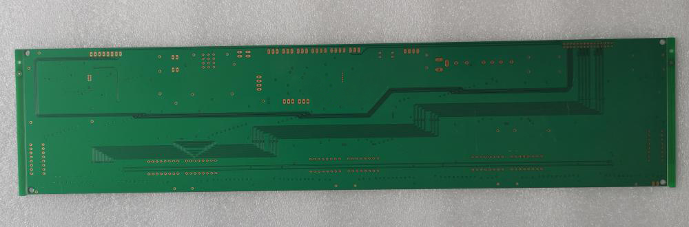
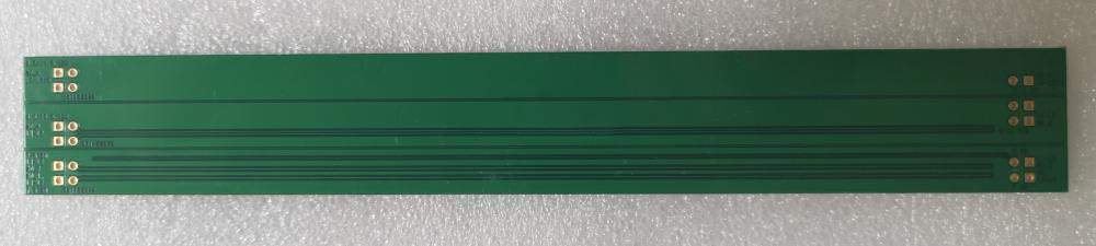
 PCB impedance control
Controlled impedance in the fabrication and design of PCB is a complex and broad topic. Therefore, understanding it could be somehow tricky.
If you are new to this, or you are searching for some information on the topic, then this guide will be of help to you. You’ll understand the hows, whys, and whats of impedance control. Please continue reading.
This is a good question. For us to understand what controlled impedance is, let us first of all define what impedance is. Impedance has to do with the degree at which the energy flow in a transmission line or electric circuit is opposed.
This is measured in Ohms and is represented as Z. This is the result when the reactance (X) and the resistance (R) are summed up. The reactance here is the result of two effects, which includes:
Usually, at DC, there is no reactance, and the copper’s resistance is typically trivial. For the high-speed AC circuits, the impedance and reactance becomes very important. Here, impedance can be critical due to the functionality of the design.
This is because impedance changes along the path of the signal from the transmitter to the receiver could lead to glitches, as well as a reduction in the performance of the system. Controlled impedance can be defined as a design technique, which assures that mismatches of the impedance in a circuit falls within limits that are tolerable.
Impedance control PCB is therefore a circuit board design having features which can control mismatches of impedance.
A PCB trace impedance comes with several features to look into concerning impedance. The features of a 50 ohm PCB trace PCB board design impedance include: dielectric constant, length, width, height, PCB fabrication limits/tolerances, and the distance between the track & other copper features.
These are the characteristics to look into when manufacturing impedance control PCBs and when calculating it.
Recently, we’ve seen a continuous rise in device switching speeds. Generally, these devices have suddenly become complicated and faster. For instance, signal integrity issues have now become very repetitive with an increase in the operational speeds of devices. This means that the devices of today must be able to solve any SI issues.
Therefore, you cannot keep treating PCB traces as point-to-point connections. Rather, begin to consider them as transmission lines. Also, you must understand the importance and necessity of impedance matching in getting rid of or reducing the effect on SI. Know that, by working with good design approaches and practice, you can easily prevent possible SI issues. In this case, controlled impedance can assist you in mitigating or averting SI issues.
Other reasons why you need impedance control PCB includes
PCB trace functions to transfer a driver device’s signal power to a device that will receive it. Here, power has to be transmitted all through the trace’s length. However, maximum signal power can only be achieved with the PCB’s matching impedances.
This is one reason why an impedance control PCB is needed. This type features an impedance matching, which permits enough power from the driver of the device and ends at the receiver.
If you are searching for a PCB, which ensures quality device performance, then you should choose impedance control PCB.
One reason why the majority of devices fail when it comes to integrity and signal power is as a result of poor PCB layout and design. The layout stage during the manufacturing of PCB is usually a very critical one. If one is not careful, there’s a high chance that there will be a degradation of high-speed signals as they propagate to the receiver.
Devices that are controlled by impedance control PCB usually utilize less energy and perform faster. This PCB type allows devices to function better for long, thereby improving their control reliability and value.
It’s true that impedance control PCB makes use of less energy. However, if you also need to control the flow of energy in your projects, then one great choice is impedance control PCB. The fact is, controlled impedance is important when transitioning from lower to higher ohm environments where there is impedance.
Why is this so? These transitions could result in reflection of energy to look like powerful and strong pulses. These pulses can disrupt the flow of energy. Therefore if your application deals with digital devices that work with high power, like those of RF applications, then it becomes necessary to use impedance control PCB.
If you use impedance control PCB, then you don’t have to worry about circuit disruptions, as a result of electromagnetic interference.
Concerning the PCB world, a pulse of reflection energy can disrupt circuits completely. This disruption usually extends to neighboring components. Also, there is a strong potential to interrupt the flow of energy and cause product operation failure.
To ensure signal integrity in PCB designs with high-speed, there’s a need for great impedance characteristics in the connections of the conductor trace.
These can only be determined after the PCB’s controlled impedance is calculated based on the impedance specifications, layout, and layer buildup.
What results is slight changes of the stackup and the relevant conductor geometries. Note that a PCB’s impedance is majorly influenced by:
Making use of simple equations, you can now calculate for controlled impedance. This will help in obtaining nominal values of impedance’ trace dimensions. These equations are very important for spacing and line widths higher than 15mil.
These simple equations are just approximations. Normally, they don’t give the best results utilized on PCBs of current technology. Besides, these equations usually need complex mathematics. Due to this reason, to determine PCB controlled impedances, utilize a PCB impedance calculator.
You can get some of these calculators online. Just choose one you can easily work with and make sure that you input the right calculation values. Remember that, whatever results are shown by these calculators are uniquely for rough estimation and approximation.
The manufacturer should calculate the corresponding layer construction, and impedance.
Usually, manufacturers of PCB will deliver standard stack up. This will be utilized to calculate, either through software or by hand, what the trace dimension be with reference to this stack up.
If your results are plausible, then make use of them. Other than this, you’ll have to indicate the stack up that suits your needs. How can this be achieved?
Begin with a practical trace thickness for manufacturability, spacing, routing. Also compute the dielectric thickness, given that there is a material with the right with a specific dielectric constant, for your required impedance.
For the right options of prepreg sheets and core thickness, make sure you pick the closest type. Immediately you achieve this, recalculate your trace dimensions. If you are using software, and it permits it, check that the SI is okay and stimulate the critical lines.
Remember that this requires trace dimensions, driver model, and stackup specifications. It will also require whichever vias you may be using, as well as their dimensions. Also, correct these accordingly; you’ll have the trace and stackup dimensions for the needed impedance.
Now, the next thing for you to do is to deliver the information to your manufacturer. To achieve this, just draw a representation of a similar thickness. You can include some notes that specify your desired dielectric material and constant.
The initial step in designing your PCB is the schematic capture. Just the same way you will draw on paper, draw a conceptual circuit. Then for each circuit’s symbol, give it a footprint. A footprint is the component’s physical package.
After the footprint is assigned, the CAD program used will generate a netlist. A netlist can be referred to as your schematic’s flat representation, which is usually machine-readable. It gives a unique ID to each footprint’s pin.
In addition, given your schematics, it creates a rundown of the connections between the nodes. At this point, you’ll be opportune to perform the layout of the actual design.
Generally, your circuit board needs to be very small. Also, you’ll want this option to suit all the connections needed at your desired widths. For this, you’ll require wider traces, because it is a high-speed circuit.
Making use of more layers means making the signal clearer is possible, as well as reducing the size of the PCB. After the layering is completed, you can then go ahead to place components beginning with those having physical constraints.
Let’s say your board has connects, LEDs, or switches, they have to be positioned to match the box’s cut out holes. You’ll then continue by placing the complicated and large ICs in a way that reduces the required traces.
At this point, you can place the different components supporting everything already explained above. Finally, you can go ahead to create traces (wires), which connect pads/pins, which should be connected. Here, CAD programs play an important role because they can check for error making use of netlist.
I hope you have been able to find answers to questions running through your mind regarding impedance control PCB. As mentioned earlier, to understand impedance as well as problems surrounding impedance control are not that easy.
Nonetheless, we have done our best to explain the topic deeply, and at this point, I believe you have become an expert on impedance control PCB.
The impedance of the circuit board is determined by the physical dimensions (line wide/space) and materials of the circuit and is measured in Ohms (Ω).
PCB impedance control has been one of the essential concerns and challenging problems in high-speed PCB design. As an impedance control designer, you should know what affect PCB impedance and how to calculate impedance.
1) Distance of signal layer and potential
2) Conductor geometry
3) Trackwidth
4) Copper thickness
5) Permittivity εr


Formula Restrictions:0.1 < w/h < 3.0

Formula Restrictions:0.1 < w/h < 3.0

Formula Restrictions:0.1 < w/h < 3.0

Formula Restrictions:0.1 < s/h < 3.0
Here is some free PCB software that provides impedance control calculations and online calculators as a reference.
Selecting Foil-Built or Core-Built PCBs to Support Impedance Control
XDF Technology normally suggests impedance designers choose Foil-Built PCBs in order to make the most economical PCB. That being said, our Prototype PCB Assembly is very flexible, and we can use Core-Built PCBs. Foil-Built PCBs not only tend to be more economical than Core-Built PCBs, but they are also slightly easier to fabricate. The pictures below explain the differences between the Foil-Built and Core-Built PCBs.


Foil-Built PCB board uses one less core than the Core-Built PCBS in the stack-up. The outside consists of aluminum foil. In addition, foil in different copper weights is much easier to purchase. Since Foil-Built PCBs are made of aluminum, they can be used on any builds, regardless of the primary laminate material used. PP (Pre-pregs) are also less costly than cores, especially if they are 5 mil or thinner.
Core-Built PCB board has cores on the outside, so there is no need to use aluminum foil. Depending on material availability, it may be difficult to acquire a core with uneven copper weights. This forces the PCB manufacturer to etch down the cores, which is costly since a good deal of labor is involved. Except for labor, the PCB factory must use a higher copper weight than what appears on the board, increasing material cost.
Nowadays, PCB designs and electronic components become smaller, faster – in other words, more complicated. PCB Impedance Control is becoming more critical. XDF has ten years of PCB manufacturing experience, and we can provide full support when designing a PCB impedance board.
The opposition encountered during current transmission in a DC circuit is called resistance, and the opposition encountered by the current in an AC circuit is called impedance. The opposition encountered by the transmission signal in the high frequency (>400MHZ) circuit is called the characteristic impedance. In high frequency, the transmission signal copper wire on the PCB can be regarded as a conductive line composed of a series of equivalent resistance and a parallel inductance. This equivalent resistance is as small as it can be ignored. Therefore, when we analyze the signal transmission of a PCB at high frequency, we only need to consider the effects of the stray distribution of series inductance and parallel capacitance. We can get the following formula:
Z0=R+√L/C√≈√L/C (Z0 is the characteristic impedance value)
With the development of science and technology, especially the advancement of integrated circuit materials, the computing speed has significantly improved. It also promotes the integration of integrated circuits towards high density, small volume, and single parts. These are the reasons that lead to a high frequency of future PCB materials. The use of high-speed digital circuits means that the impedance of the circuit must be controlled, low distortion, low interference, low crosstalk, and elimination of electromagnetic interference (EMI). Impedance design is gradually crucial in PCB design. In PCBs with high-frequency signal transmission, the control of characteristic impedance is critical, and characteristic impedance is the core of solving signal integrity problems. At the front-end of PCB manufacturing, the front part of the system is responsible for the simulation calculation of impedance and the design of the impedance bar. Customers have become more stringent in impedance control. The number of impedance controls has increased how to quickly and accurately design impedance is a problem that greatly concerns PCB designers.

Impedance(Z0) definition: The total opposition to an alternating current flowing through it at a known frequency is called impedance(Z0). For PCBs, it refers to the total opposite of a certain circuit layer (signal layer) to its closest reference plane under high-frequency signals.
In electronic information products such as computers and wireless communications, the energy transmitted in the PCB circuit is a square wave signal composed of voltage and time. The opposition it encounters is called characteristic impedance.
Two identical signal waveforms with opposite polarities are input at the driving end, respectively transmitted by two differential lines, and the two differential signals are subtracted at the receiving end. Differential impedance is the impedance between two lines.
The impedance of one line to the ground is the same as the second line.
Impedance when two same signal waveforms with the same polarity are input at the drive end, and the two wires are connected.
The impedance of one of the two lines to the ground is the same as the impedance of the two lines; it is usually greater than the odd mode impedance.
Among them, characteristic impedance and differential impedance are common impedance, and common-mode impedance and odd-mode impedance are rare.
W — Line width/line space: The line width increases, the impedance decreases, and the distance increases, the impedance increases.
H — Insulation thickness: the thickness increases, and the impedance increases.
T — Copper thickness: the copper thickness increases, and the impedance decreases.
H1 — Solder mask thickness: the thickness increases, and the impedance decreases.
Er — The dielectric constant: the DK value increases, and the impedance decreases.
Undercut — W1-W: the undercut increases, and the impedance increases.
In addition, when the surface process is immersion-gold (or gold plating), the etching process of the outer layer is different from other surface processes, and the line compensation is different. The impedance calculation result of the former will be 3-5 ohms larger, so the resistance value of the gold plating process and other process switching needs to be adjusted.
The most commonly used impedance calculation tool in our industry is the Si8000 Field Solver provided by Polar. Si8000 is a brand-new boundary element method field-effect calculator software. It is based on the easy-to-use user interface of the early Polar impedance design system we are familiar with. This software contains various impedance modules, and personnel can calculate impedance results by selecting specific modules, inputting related data such as line width, line spacing, inter-layer thickness, copper thickness, and Er value. A PCB impedance control number can be as few as 4 to 5 groups or as many as dozens of groups. The control line width, inter-layer thickness, copper thickness, etc., of each group are also different. If you check the data one by one and then manually input the relevant parameters and then calculate, it is time-consuming and error-prone.
To ensure the quality of signal transmission, reduce EMI interference, and pass relevant impedance testing and certification, it is necessary to conduct an impedance matching design for PCB key signals. Considering common calculation parameters, TV product signal characteristics, PCB Layout actual needs, SI8000 software calculations, PCB supplier feedback information, etc., finally come to this recommended design. It is suitable for most PCB suppliers’ process standards and PCB board design with impedance control requirements.
100 ohm differential impedance recommended design
90 ohm differential impedance recommended design
Note: Prioritize the use of package ground design. However, if the line is short and there is a complete ground plane, it can be designed without package ground.
Calculation parameters:
FR-4, thickness 1.6mm+/-10%, dielectric constant 4.4+/-0.2, copper thickness 1.0 oz (1.4mil), solder mask thickness 0.6±0.2mil, dielectric constant 3.5+/-0.3.

Fig.1 Design of ground package Fig.2 Design without ground package
100 ohm differential impedance recommended design
line width, spacing 5/7/5mil differential pair and the distance between the pair ≥ 14mil (3W criterion);
Note: It is recommended that the entire group of differential signal lines is shielded with ground, and the distance between the differential signal and the shielded ground line is ≥35mil (in special cases, it cannot be less than 20mil).
90 ohm differential impedance recommended design
line width, spacing 6/6/6mil differential pair, and the distance between the pair ≥12mil (3W criterion).
Note: In the case of a long differential pair trace, it is recommended that the USB differential line wrap the ground at a distance of 6 mils on both sides to reduce the risk of EMI (with and without ground, the line width and line spacing standards are consistent).

Calculation parameters:
FR-4, thickness 1.6mm+/-10%, dielectric constant 4.4+/-0.2, copper thickness 1.0 oz (1.4mil), copper clad substrate(PP) 2116 (4.0-5.0mil), dielectric constant 4.3+/-0.2, solder mask thickness 0.6±0.2mil, dielectric constant 3.5+/-0.3.
Stack-up:
| Silkscreen |
| Solder mask |
| Copper |
| Prepreg |
| Base material |
| Prepreg |
| Copper |
| Solder mask |
| Silkscreen |
The impedance design of the outer trace is the same as that of the four layer board.
The inner trace is generally more plane layer than the surface trace, and the electromagnetic environment is different from the surface.
The following is the third layer trace impedance control recommendation.
100 ohm differential impedance recommended design
line width, spacing 6/10/6mil.
The distance between the differential pair is ≥20mil (3W criterion).
90 ohm differential impedance recommended design
line width,line spacing 8/10/8mil.
The distance between the differential pair is ≥20mil (3W criterion).

Calculation parameters:
FR-4, thickness 1.6mm+/-10%, dielectric constant 4.4+/-0.2, copper thickness 1.0 oz (1.4mil), copper clad substrate(PP) 2116 (4.0-5.0mil), dielectric constant 4.3+/-0.2, solder mask thickness 0.6±0.2mil, dielectric constant 3.5+/-0.3.
Stack-up:
| Silkscreen |
| Solder mask |
| Copper |
| Prepreg |
| Base material |
| Prepreg |
| Base material |
| Prepreg |
| Copper |
| Solder mask |
| Silkscreen |
Note:
PP types
| Type | Dielectric thickness | Adjustable range | Dielectric constant |
| 1080 | 2.8mil | 2.0-3.0mil | 4.3 |
| 2116 | 4.2mil | 4.0-5.0mil | 4.3 |
| 1506 | 6.0mil | 5.5-6.5mil | 4.3 |
| 7628 | 7.2mil | 7-8.5mil | 4.3 |
Solder mask thickness: 0.6±0.2mil
Cer=3.5+/-0.3

Impedance test receives the reflected wave simultaneously after the oscilloscope sends out a pulse wave, then compares and analyzes the two pulse waves, and gets the impedance value from the reflected energy.

Impedance test schematic
Using TDR (Time Domain Reflectometry) measurement, the general measurement method uses “time domain reflectometry.”
The calculation formulas of some impedance types are introduced above, but the current impedance is calculated by the software, which is faster and more accurate. Our factory currently uses Polar’s test instrument CITS500s.
Test range: 0-300ohm
Test accuracy: 1%—50ohm
1.25% — 75ohm
1.5% — 28\100ohm
Reflected Pulse Rise time: ≤200ps
System bandwidth: 1.75GHz
The dielectric constant Er will change with the working frequency. Within a specific range, the higher the frequency, the smaller the Er. Annex I, Annex II, and Annex III are core board Er provided by three sheet suppliers, which can be viewed at 1MHz. The dielectric constant is greater than that at 1GHz.
It is composed of resistance and reactance (combined by inductive reactance and capacitive reactance). The characteristic impedance in the PCB depends on the width and thickness of the wire, the distance between the wire and the ground plane, and the dielectric constant (εr) of the medium between the wires.
The signal transmission in the electronic circuit starts from the output of the power supply. It expects to be transmitted to the receiving end without energy loss and any signal reflection in the middle.
Therefore, the impedance (ZL) in the PCB is required to be equal to the impedance (ZO) of the power supply terminal, which is called impedance matching. If the impedance cannot be matched, the received signal is distorted.
A transmission line structure in which the wires are parallel to the ground plane in the PCB and separated by the medium.
A strip-line is a high-frequency transmission wire between two parallel ground planes (or power planes) between dielectrics.
In the circuit, the ratio of voltage to current in the transmission wave between two points, including the assembled components, is the resistance of any point of the transmission line to the transmission wave.
For non-coplanar type impedance bars, if the customer does not specify requirements when designing the impedance bar, the Dummy Pattern next to the signal line (the distance between the long copper bar or copper pad and the signal line, t, must be ≥5H (H is the signal layer to the shield) The insulation thickness or minimum thickness of the layer). The following examples illustrate.
Note: For non-coplanar type impedance, when the distance between the Dummy Pattern and the copper skin is less than 5t, the impedance will become smaller as the distance becomes smaller
C4 Jinxiongdakejiyuan Huanguannan rd, Guanhushequ, Longhua district Shenzhen China
 sales@pcba360.com
 PCBA360
 +86-755-84717796
Certifications

Delivery


<

 Quote
Quote