
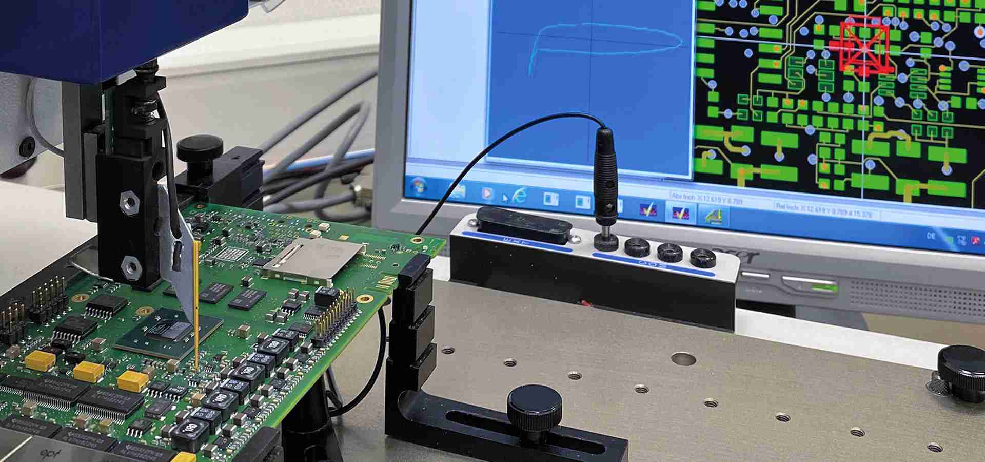
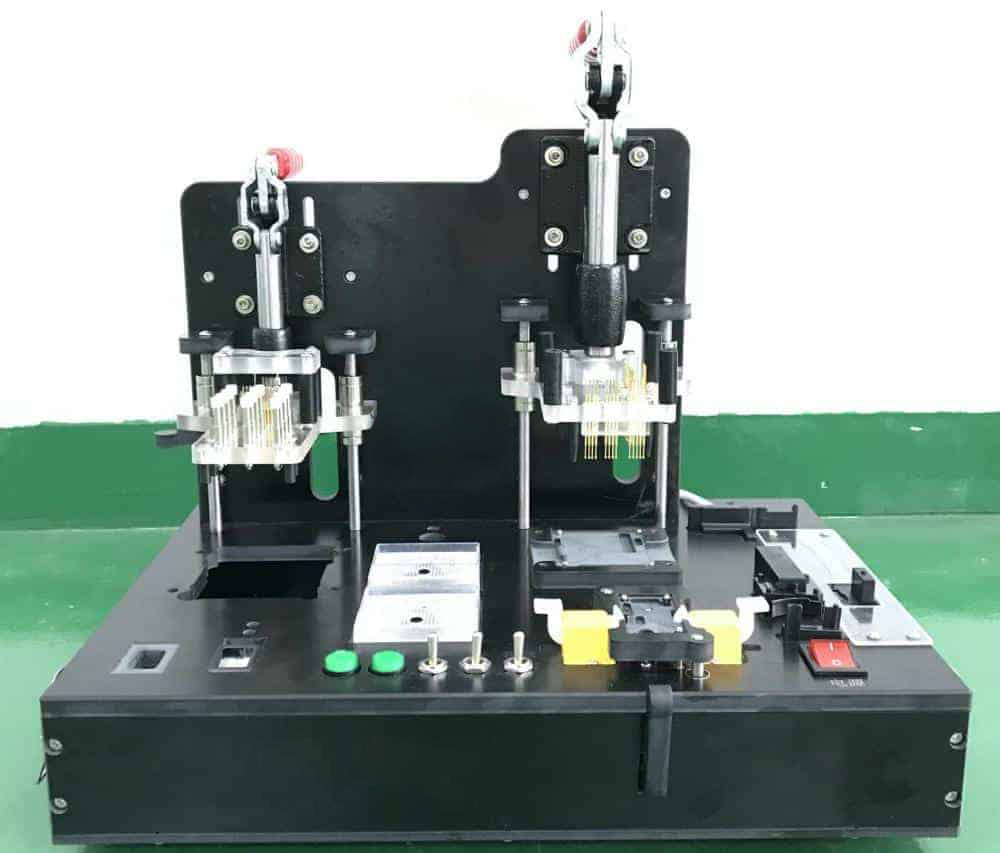
In-Circuit Test will ensure 100% quality pass, When design your board, Pls request
electronic engineers to pre-design ICT, We will use diagram to make ICT fixture,
and 100% testing before shipping
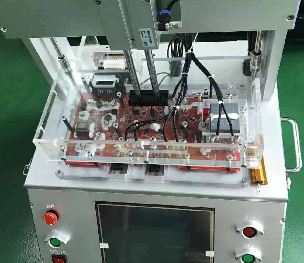
In-Circuit Test (ICT) is a standard test method to check the PCBA manufacturing defect and poor component by testing the electrical performance and connections of circuit components.
It mainly checks the in-circuit individual components and the open and short circuit conditions of each circuit network. It has the characteristics of simple operation, fast and rapid, and accurate fault location.A good electronic engineer will pre-consider test point when designing a PCB.
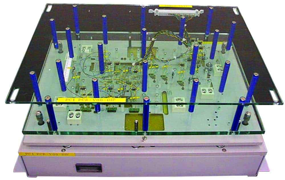
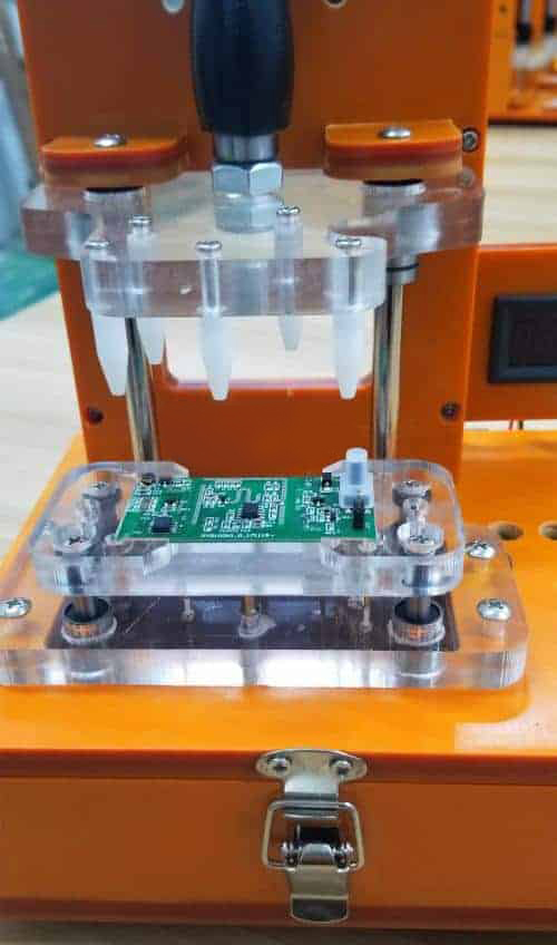
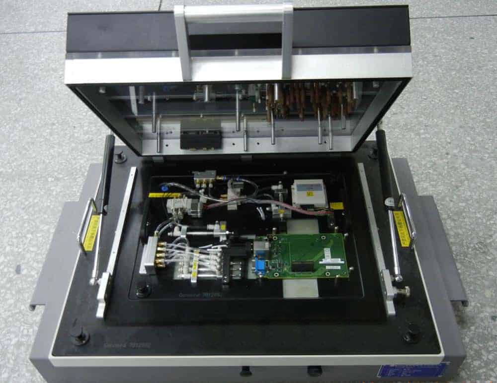
ICT Needle-bed can test analog device functions and logic functions of digital devices and has a high fault coverage rate. However, special needle-bed fixtures need to be made for each type of single PCB board, and the fixture production and program development cycle is long.
(1) It can detect all the parts on the assembled circuit board in just a few seconds,such asresistors, capacitors, inductors, transistors, FETs, LEDs, ordinary diodes, stabilized diodes, optocouplers, ICs, etc. It also checks whether the part works within the specifications of the design.
(2) It can determinethe PCBA manufacturing process defects in advance, such as short circuit, open circuit, missing parts, reverse, wrong parts, empty welding, etc.Then it provides feedback to the improvement of the process.
(3) The faults mentioned aboveor test results can be printed out, including the location of the fault, the standard value of the part, and the test value for reference by the maintenance personnel. It can effectively reduce the personnel’s dependence on product technology. Even if the personnel is not experienced with PCB circuits, they are still able ability to contribute.
(4) It can determinethe failed test, and the production management personnel can analyze the information to determine the causes of defects, including human factors. This is so that they can resolve, correct and improve the circuit board manufacturing and quality capabilities.
The electrolytic capacitor is reversed, and the missing parts are 100% testable Parallel electrolytic capacitors are reversed, and the missing parts are 100% testable The working principle of electrolytic capacitor polarity test technology:
1.1 It is to use the third pin to apply a trigger signal to the top of the electrolytic capacitor and measure the response signal between the third point and the positive or negative terminal.
1.2 After calculating with DSP (digital signal processing) technology, it is converted into a set of vectors through DFT (Discrete Fourier Transform) and FFT (Fast Fourier Transform). The resulting response signal is converted from t(time) domain (oscilloscope signal) to f(frequency) domain (spectrum analyzer signal) vector group.
1.3 Getting a set of standard vector values through learning, and then the measured value of the DUT (Device Under Test) is compared with the original standard value through Pattern Match (feature recognition and comparison technology) to determine whether the polarity of the test object is correct or not.
Pattern Match is used in applications such as fingerprint recognition, counterfeit currency recognition, retina recognition, etc.
That is Short:10Ω, Lr:20Ω, Open:80Ω. This standard is the system default setting and can be changed if needed.
There are two types of circuits that are helpful in electronic measurement: 1. To generate measurement parameters (voltage and current). 2. To control the existing voltage and current in the circuit.

When measuring resistance Rx with multimeter
∵Lx=Is-I1≠Is ∴Vx/Is≠Rx
If the potential Va at point A is sent to point G, let Vg=Va Ir1=(Va-Vg)/R1
∴Ir1=0 Is=Ix ∴ Rx=Vx/Is
Resistance measurement is the extrapolation from voltage and current measurements. The ohm meter itself must provide an excitation source for the boards under test. The resistance can be measured without being part of the circuit. Suppose the resistance is part of the circuit.
In that case, other voltage or current sources must be removed, and the power supply or battery must be turned off or disconnected from the circuit. Otherwise, the current or voltage will have the reading incorrect.
DC constant current source: According to Ohm law: V=IR,we get Rx=Vx/Is。
Therefore, Rx can be calculated by measuring the AB terminal voltage Vx.
(Constant current range: 0.1UA-50MA)

Resistor R/C(MODE V5,CV)
DC constant voltage source: According to Ohm law: V=IR,we get Rx=Vs/Is=0.05V or 0.1V/I
Therefore, if Ix is obtained, the Rx value can be calculated.
Vs=0.1v, 0.05v

Resistor R/L(MODE P1、P2、P3、P4、P5)
Phase method test: AC voltage must Vs, assisted by phase method Rx=1/|Y`|Cosθ

Resistor R (MODE XR)
25V voltage source, measure the resistance above 1M
AC constant voltage: AC voltage must be Vs, Vs/Lx=Zc=1/2πfCx
Get: Cx=Ix/2πfVs

*Capacitance C/R (MODE P1 P2 P3 P4 P5)
Phase method test: |Y`|Sinθ=|Ycx|, ie ωCx’Sinθ=ωCx
Get: Cx=Cx’Sinθ (Cx’=Ix’/2πfVs)

*Capacitance C 3UF or more large capacitance (MODE DC)
DC constant current: C=ΔT/ΔV*I
*Inductance L (MODE A1 A2 A3 A4 A5)
Vs/Ix=Zl=2πfLx get: Lx=Vs/2πfIx

Phase testing :|Y`|Sinθ=|Ycx|,即Sinθ/ωCx’=1/ωCx get:Lx=Lx’/ Sinθ ( Lx’=Vs/2πfIx’)


Diode
A diode is a two-terminal component. When it is reverse biased, the anode voltage is negative relative to the cathode, and it has a high resistance. When it is NPN, it presents voltage drop and low resistance. The drop of forward voltage is related to the type of diode, usually less than 1V. Silicon: 0.6v-0.7v, germanium tube: 0.25-0.4v, Schottky block type: 0.4-0.5v, LED: 1.5-2.5v.
When measuring the diode, Vs should be bigger than the forward voltage drop of the diode. But it should not be too big to avoid excessive voltage or diode damaged by the current. NPN test: The general voltage source is 2.2V, and then measure its voltage. Forward direction: about 0.7v, reverse direction: 2.2v. The forward voltage drop of a diode is related to the diode type and is usually less than 1V.
Silicon: 0.6v-0.7v, germanium tube: 0.25-0.4v, Schottky barrier type: 0.4-0.5v, LED: 1.5-2.5v.
There are three methods to test IC in ICT test: IC clamping diode test, IC scan, and IC test jet. Among these three test methods, the IC clamping diode test is the most commonly used, and most of the tests have this function. The IC scan function is a test program developed by PTI to the blind spots in IC testing. The IC test jet is a test solution developed by Agilent TestJet Technology to solve the problem of SMD IC pin open in circuits. It is used for IC open joint test.
The IC Clamping Diode test method tests the low voltage function with each IC pin to the IC VCC PIN, or with each IC pin to the IC’s GND PIN, or with the two adjacent IC pins as the two test points.
The test program is generated by the automatic learning method. When making a program, use the software IC’s Pin Edit function to put into the corresponding probe number of each pin of the IC, and specify which PIN is VCC PIN and GND PIN
The test principle: Test according to the protection diode of each pin in the IC manufacturer’s footprint to GND/VCC, which can assist in the IC empty welding and reverse test.
IC SCAN technology checking SMD IC pin open circuit (PIN OPEN) method because each pin is tested by the three pins of the IC, so even the pin on the Bus can also be checked.

Its principle as shown in the figure:
step 1: A= –0.9v B=0v measure current,get: I1=I3+I4
step 2: A= –0.9v B= –1.2v Measure current, get: I2
step 3: I=I1-I2 I>0 get Good I≤0 get Bad
Note:
In order to conduct the test, the IC test jet uses the sensor plate on the fixture to press on the IC; the sensor plate’s shape and area are the same as the IC shell. Then use the capacitance between the sensing board’s copper foil and the IC foot frame to check the open circuit of the pin. The system sends a 200mV, 10KHz signal from the test point to the IC pin.
The signal passes through the capacitive coupling between the IC frame and the sensing board, then through the amplifier on the sensing board. Go to the 64 channel signal conditioning card to select and amplify the signal, and finally connect to the test jet system to measure the signal strength. If the IC pins have open, as the signal could not be detected, the system will know that it is an open circuit.
The PTI816NT ICT system is equipped with this technology, which significantly improves the detectability rate of digital circuit boards. Computer motherboard, adapter card, fax machine, and modem board can all get satisfactory test results. Agilent Testjet Technology can also detect the open circuit of various socket pins, whether it is Insertion type or SMD type. As shown below:
Judging from the current application situation, test methods that combine two or more technologies are becoming a development trend.

Different ICT testing technologies have advantages and disadvantages. By combining IC clamping diode test and IC scan technology, they do not need additional test accessories. IC scan is a free additional function of PTI and not affected by IC packaging/height and can test the parallel connection of ICs, especially for IT products such as motherboard BGA, sound card, display card. On the other hand, IC scan and test jet technology are mainly aimed at SMD IC testing its empty solder, cold solder, etc.
IC test jet confirms whether the component exists, but it cannot confirm whether the components, directions, or values are correct. Using two or more test methods can reduce the ICT test failure rate.
The PTI816 series measuring board use a four-layer board structure, they are:
DC Board: DC signal source, measuring resistance, diode, triode
AC Board: AC signal source, measuring capacitance and inductance
SYS Board: Control and conversion of input and output signals
IC Scan Function Board: System self-check, IC scan function, test jet function test
System self-diagnosis and debug function
TESTSELF.STD is a system self-test program, which includes some resistance, capacitance, and inductance.
*If the self-inspection finds that the resistance test or the voltage of 1V, 4V, 8V, or 24V failed, it means that the DC board is damaged.
*If there is a problem with a single resistor, it means that a certain gear on the DC board is not functioning properly.
*If the capacitor or inductance is poor in self-check, the AC board is damaged. If a certain capacitor or inductance is bad, the corresponding gear of the AC board is broken.
*If the SYS Board is damaged, all component tests will fail.
When Relay Board self-checking, “MPX OK” will be displayed on the fluorescent screen. Otherwise, it will show that the corresponding switchboard’s relay board is broken, such as: Open or Short.

If one or two abnormalities are found above, please make necessary relevant records and notify PTI as soon as possible.
Appendix 4: Ceramic capacitor error:
F:±1% R:-20% +100%
G:±2% S: 0% +20%
H:±2.5% T:-10% +50%
J:±5% Z:-20% +80%
K:±10% M:±20%
★ Debug Sequence of Debug program:
Then turn on the photoelectric protection switch.
Why Debug? When the new program is in actual SCAN, due to the selection of signal, the influence of component circuit or loop, and the error of the test pin number, few steps will be bad (the measured value exceeds ±%).
R debugging: According to the size of R, the system automatically adjusts the value of the test current. (0.1UA-50MA)
F9: Single-step debugging ALT+F9: Whole page debugging F5: Swap AB point
F10: Automatic Guarding ALT+H: View series components
ALT+J: View parallel components, select corresponding MODE and AB points
R/C: CV V5 and Dly(TM)
R/D: D2 V5
R/R: STD value is the parallel resistance
R/L: P1, P2, P3, P4, P5; According to Zx=2πfL, when L is constant if f is bigger, Zx is larger, and the influence on R is smaller.
C debugging: 3uf to 300uf, the system signal source is both AC and DC, above 300uf is DC Mode, small capacitors below 470pf are A4 A5 and OFFSET, 470pf to 3uf A3 A2 A1
F9: Single-step debugging ALT+F9: Whole page debugging F5: Swap AB point
F10: Automatic Guarding ALT+H: View series components
ALT+J: View parallel components, select the corresponding MODE and point A and B
C/C: STD value is the parallel capacitance value
C/R: A1, A2, A3, A4, A5; According to Zc=1/2πfC, when C is constant, the higher f is, the smaller Zc is, and the smaller the influence of R is.
C/L: P1, P2, P3, P4, P5; According to Zx=2πfL, when L is constant, if f is higher, Zx is larger, and the influence on C is smaller.
C/D: DC AB position A1, A2, A3, A4, A5 can conduct a good test.
D, Q, IC debugging: F9: single-step debugging ALT+F9: full page debugging
F5: Swap point AB
Forward: about 0.7V (NPN) Reverse: more than 2V (reverse cut-off)
D/C: LV add voltage and Dly
D/D: In addition to the forward conduction test for CM, a current test is also required.
Zener debugging: ACT value is bigger than Zener breakdown voltage +30%- +50%. If the test does not show the breakdown voltage, you can increase the gear and add Dly, and the Zener of 10V-48V can use HV.
The ce pole of Q: Need to confirm the type of Q (NPN, PNP), point A is the same (NPN), and point B is the same (PNP)
In order to make ce extremely saturated and conductive, the bias voltage of NPN is 0.6v-1v, and the bias voltage of PNP is 2.5v-1.8v. The reverse cutoff is above 0.5v (otherwise, adjust the ACT value).
Special test method:
Voltage regulator 7805:
Small resistance four-wire measurement: 1. When measuring minimal resistance, the resistance of the probe and the cable may introduce significant errors. The current Is flows through these stray resistances and generates a voltage across the resistance.
Because the voltmeter contains R1 and R2 voltage in the measurement, the stray resistance added to the unknown resistance Rx will cause errors.
Different manufacturers: Agilent Technologies, Teradyne, POSSEHL, SAMSUNG(FARA), T2000, GW, SEICA, WINCHY, TAKAYA, Check Sum (USA), Hioki, IFR, Takaya (Japan), Tescon, Okano(Japan), Rohde & Schwarz, Scorpion, Shindenski, SPEA, Tecnost-MTI, Testronics, SYS (Taiwan Series), Tr, WK Test, JET, Schuhll, Viper, TTI, SRC, Hong Kong Concord, etc. have applications in China.
Agilent hp3070, Teradyne, and Winchey have the highest market recognition among them.
The flying probe ICT only does static testing. The advantage is that no fixtures are required, and the program development time is short. Needle-bed ICT can test analog device functions, digital device logic functions, and a high fault coverage rate. However, special needle-bed fixtures must be made for each type of single board, and the fixture production and program development cycle is long.
Scope and characteristics: Check the electrical performance of in-circuit components and the connection of the circuit network. Firstly, it can quantitatively measure resistance, capacitance, inductance,
C4 Jinxiongdakejiyuan Huanguannan rd, Guanhushequ, Longhua district Shenzhen China
 sales@pcba360.com
 PCBA360
 +86-755-84717796
Certifications

Delivery


<
 Quote
Quote