
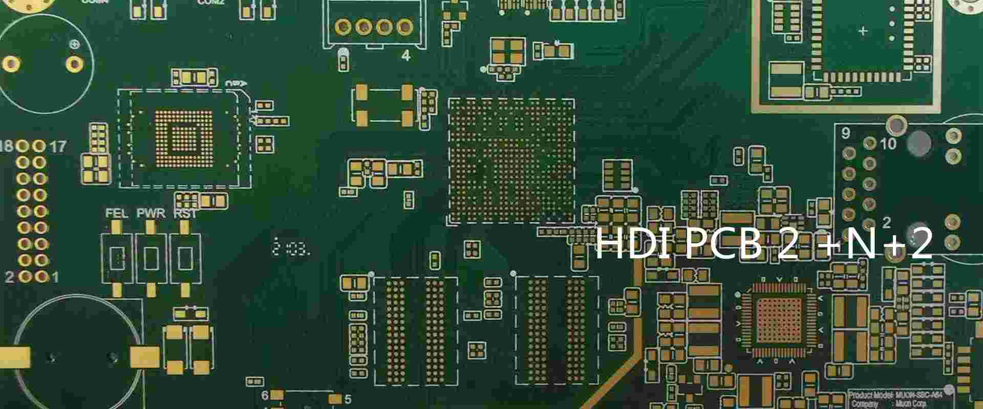
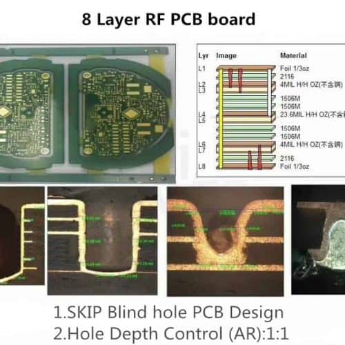
HDI technical: 1+N+1, 2+N+2, 3+N+3,4+N+4, any layer in R&D
High Quality high-density interconnect PCB Manufacturing, blind via or/and buried hole, accept any layer of the PCB to be interconnected freely.
XDF is 15 years HDI PCB manufacturer, Send Your HDI Design file to Sales@pcba360.com, Esimate Cost Now !
HDI PCB Manufacturing Capabiltiy : 1+N+1, 2+N+2, 3+N+3,4+N+4, any layer in R&D
HDI PCB is the short form of high-density interconnect printed circuit board, a kind of printed circuit board manufacturing technology. An HDI PCB is a circuit board with a relatively high circuit density that uses micro-blind and buried “via”—or the copper-plated holes in PCBs—technology. HDI PCB are compact products designed for small-capacity users, as they cost much more than standard PCB.
HDI PCB boards, one of the fastest growing technologies in the PCB industry, are now available at XDF Technology. HDI PCB contain both the blind via and buried via hole varieties and have a higher circuitry density than traditional circuit boards.
The following is a breakdown of the various structures offered by XDF:
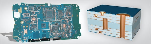
4. Any Layer HDI – All the layers of a PCB are high-density interconnection layers, which allows the conductors on any layer of the PCB to be interconnected freely with copper-filled stacked microvia structures (“any layer via”). This provides a reliable interconnect solution for highly complex, large pin count devices, such as central processing unit (CPU) and graphics processing unit (GPU) chips utilized on handheld and mobile devices.
A microvia maintains a laser-drilled diameter of, typically, 0.006″ (150µm), 0.005″ (125µm), or 0.004″ (100µm), which are optically aligned and require a pad diameter of typically 0.012″ (300µm), 0.010″ (250µm), or 0.008″ (200µm), allowing additional routing density. Microvias can be via-in-pad, offset, staggered or stacked, non-conductive filled and copper-plated over the top, or solid copper filled or plated. Microvias add value when routing out of fine-pitch ball grid arrays (BGAs) such as 0.8 mm pitch devices and below.
Additionally, microvias add value when routing out of a 0.5 mm pitch device where staggered microvias can be used. However, routing micro-BGAs such as a 0.4 mm, 0.3 mm, or 0.25 mm pitch device, requires the use of Stacked MicroVias using an inverted pyramid routing technique.
Any PCB layer Connect HDI
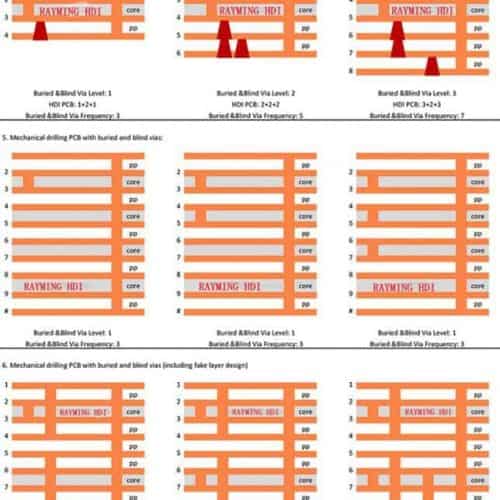
1. Multilayer copper-filled stacked micro via structure
2. 1.2/1.2 mil line/space
4/8 mil laser via capture pad size
1. High temperature FR4 (Fiberglass PCB substrate material)
2. Halogen-free
3. High Speed (low loss)
4. First Generation microvias
1. Create routing density (eliminated through vias)
2. Reduced layer count
3. Enhance electrical characteristics
4. Standard microvias limited to layers 1 – 2 & 1 – 3
1. Allows increased routing on multiple layers
2. Provides routing solutions for next generation applications
1 mm – 0.8 mm – 0.65 mm – 0.5 mm – 0.4 mm – 0.3 mm & 0.25 mm
3. Provides solid copper plate, eliminating potential solder voiding
4. Provides a thermal management solution
5. Improves current carrying capability
6. Provides a planar surface for BGAs (va-in-pad)
7. Allows any layer via technology
1. Those with through vias from surface to surface
2. Those with buried vias and through vias
3. Those with two or more HDI layer with through vias
4. Those with passive substrates and no electrical connection
5. Those with coreless construction using layer pairs
6. Those with alternate coreless constructions constructions using layer pairs
HDI any-layer connect printed circuit boards are the next technological enhancement of HDI microvia PCBs: all the electrical connections between the individual layers consist of laser-drilled microvias. The main advantage of this technology is that all the layers can be freely interconnected. To produce these HDI PCBs, XDF uses laser-drilled microvias electroplated with copper.
1.HDI technology can reduce the cost of PCB, although when the density of PCB increases beyond eight layers, it will be more expensive to manufacture with HDI.
1.The traditional and complex pressing process is low.
2.Increased circuit density: traditional circuit boards and parts are interconnected
3.Conducive to the use of advanced construction technology
4.Have better electrical performance and signal accuracy
5.Better reliability
6.Can improve thermal properties
7.Can improve radio frequency interference/electromagnetic wave interference/electrostatic discharge (RFI/EMI/ESD)
8.Greater design efficiency
Q:Can XDF manufacture a pcb with both blind and buried vias ?
A:Yes,We can manufacture any layer blind with or cross buried hole connect PCB,Send your PCB design file to get quote now !
Q:How long can I get quotation ?
A:You can get quote 24hours , If Blind cross buried hole will take 48 hours to quote.
Q:How do you guarantee quality ?
A:XDF have more than 15 years hdi pcb manufacturing experience ,All board will test 100% incluing flying proble and aoi
While advancements in electronic design continue to improve the performance of the whole device, the trend is also moving towards reducing its size. In small portable products ranging from mobile phones to smart weapons, “small” is an eternal pursuit. High-density interconnect (HDI) technology can make terminal product designs more compact, while meeting higher standards of electronic performance and efficiency. HDIs are widely used in mobile phones, digital cameras, MP3s, MP4s, notebook computers, automotive electronics ,and other digital products, among which mobile phones are the most widely used. HDI boards are generally manufactured by the build-up method.
The greater the build-up times, the higher the technical level of the board. Ordinary HDI boards are basically one-time build-up. High-end HDIs use two-time, or more, build-up technology. At the same time, advanced PCB technologies such as stacking holes, electroplated hole filling, and laser direct drilling are used. High-end HDI PCB boards are mainly used in 3G, 4G, and 5G mobile phones, advanced digital cameras, IC carrier boards, etc.
Assuming the upward trend of high-end HDI PCB boards, 4G boards, or IC carrier boards continues, future growth is expected to be very rapid: the world’s 5G mobile phone use will grow by more than 50% in the next few years, and China will issue 5G licenses. Moreover, IC carrier board industry consulting agency Prismark predicts that China’s forecast growth rate from 2020 to 2030 will be 80%, which is microcosmic of the direction of PCB technology development.
The continuous growth of mobile phone production is driving the demand for HDI PCB boards. As a technology-driven country, China plays an important role in the world’s mobile phone manufacturing industry. Since Motorola fully adopted HDI boards to manufacture mobile phones in 2002, more than 90% of mobile phone motherboards have adopted HDI PCBs.
However, China’s HDI PCB production capacity cannot meet the rapidly growing demand. In recent years, the global HDI mobile phone board production situation has undergone major changes: major European and American PCB manufacturers, in addition to the well-known mobile phone board manufacturers ASPOCOM and AT&S, still supply second-order HDI to Nokia. In addition to mobile phone boards, most of the HDI production capacity has been transferred from Europe to Asia. Asia, especially China, has become the world’s main supplier of HDI boards.
In addition to smart phones, tablet and desktop manufacturers are striving to achieve miniaturization. All these size reductions depend on the design and use of HDI PCBs. The functions of HDI technology are designed to make smart devices lighter, smaller, thinner, and more reliable.
HDI PCB refers to a printed circuit board that has high density, fine lines, small drill diameters, and are ultra thin. This kind of PCB has developed rapidly on the basis of emerging advantages, outlined in what follows.
Some new requirements are being put forward for HDI PCB materials, including better dimensional stability, antistatic mobility, and non-adhesives. The typical material of HDI PCBs is Resin-Coated-Copper (RCC). There are three types of RCCs—namely, polyimide metallized film, pure polyimide film, and cast polyimide film.
The advantages of RCCs include: small thickness, light weight, flexibility and reduced flammability, compatibility characteristic impedance, and excellent dimensional stability. In the HDI multi-layer PCB process, instead of the traditional adhesive sheet and copper foil as the insulating medium and conductive layer, the RCC can be suppressed with the chip using traditional suppression technology. Non-mechanical drilling methods such as lasers are then used to form microvia interconnections.
RCC promotes the development of PCB products from surface mount technology (SMT) to chip-scale packaging (CSP), from mechanical drilling to laser drilling—and promotes the development and progress of PCB microvias, all of which have become RCC’s leading HDI PCB material.
In the actual PCB manufacturing process, for the selection of RCC, there are usually FR-4 standard Tg 140C, FR-4 high Tg 170C, and FR-4 and Rogers combined lamination, which are mostly used now. Given the development of HDI technology, HDI PCB materials must meet more requirements. Therefore, the main trends of HDI PCB materials are:
1.Development and application of flexible materials without adhesives;
2.The thickness of the dielectric layer is small and the deviation is small;
3.The development of LPIC;
4.The dielectric constant is getting smaller and smaller;
5.The dielectric loss is getting smaller and smaller;
6.High welding stability; and
7.Strictly compatible with coefficient of thermal expansion (CTE).
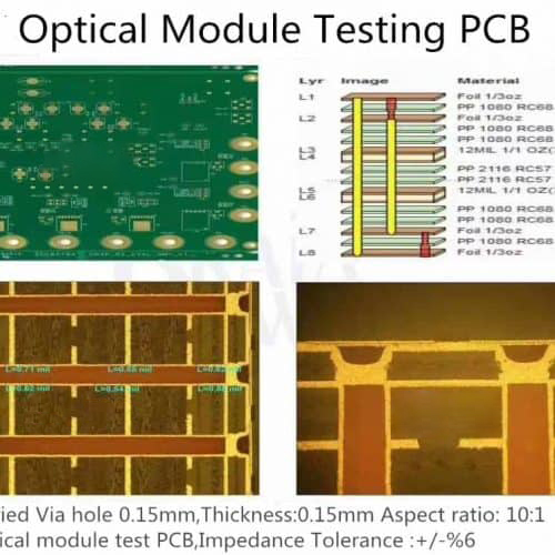
The difficulty in HDI PCB manufacturing is microvias, which are made through metallization and thin wires.
Microvia manufacturing has always been the core issue of HDI PCB manufacturing. There are two main drilling methods:
1.Mechanical drilling, which for ordinary through hole drilling is always the best choice for its high efficiency and low cost. With the development of machining capabilities, its application in microvias is also constantly developing.
2.Laser drilling, of which there are two types: photothermal ablation and photochemical ablation. The former refers to a process by which the operating material is heated to melt and evaporate through the formed through hole after the high-energy laser is absorbed. The latter refers to the result of high-energy photons and lasers exceeding 400nm in the ultraviolet region.
There are three types of laser systems applied to flexible and rigid boards, namely excimer lasers, ultraviolet laser drilling, and CO2 lasers. Laser technology is not only suitable for drilling, but also for cutting and forming. Some manufacturers even use lasers to manufacture HDIs.
Although the cost of laser drilling equipment is high, they have higher precision as well as stable and mature technology. The advantages of laser technology make it the most commonly used method in blind/buried through hole manufacturing. Today, 99% of HDI microvias are obtained by laser drilling.
The biggest challenge of through-hole metallization is that it is difficult to achieve uniform plating. For the deep-hole electroplating technology of microvias, in addition to the use of an electroplating solution with high dispersibility, the plating solution on the electroplating device should be upgraded in time. This can be done through strong mechanical stirring or vibration, ultrasonic stirring, and horizontal spraying. In addition, the humidity of the through-hole wall must be increased before plating.
In addition to process improvements, HDIs’ through-hole metallization method has also seen major technological improvements: these include chemical plating additive technology, direct electroplating technology, etc.
The realization of thin lines includes traditional image transmission and direct laser imaging. Traditional image transfer is the same as the process of forming lines by ordinary chemical etching.
For direct laser imaging, no photographic film is needed, and the image is formed directly on the photosensitive film by laser. The ultraviolet (UV) lamp is used for operation, so that the liquid anticorrosion solution can meet the requirements of high resolution and simple operation. No photographic film is needed to avoid adverse effects associated with film. CAD/CAM can be directly connected to shorten the manufacturing cycle and make it suitable for limited and multiple production.
HDI stands for high-density interconnect, a type of manufacturing printed circuit board (PCB). The PCB is a structural element formed by insulating materials and conductor wiring. When printed circuit boards are assembled into final products, integrated circuits, transistors (transistors, diodes), passive components (such as resistors, capacitors, connectors, etc.) and various other electronic parts are mounted on them.
With the help of wire connection, it is possible to form an electronic signal connection and function. Therefore, PCB is a platform that provides component connection and is used to accept the substrate of the connected parts.
Since the printed circuit board is not a general terminal product, the definition of the name is slightly confusing. For example, the motherboard for personal computers is called the motherboard and cannot be directly called the circuit board. So, when evaluating the industry, the two are related but not the same. Another example: because there are integrated circuit components mounted on the circuit board, the news media calls it an integrated circuit board (IC board), but in essence it is not equivalent to a printed circuit board.
Given the premise that electronic products tend to be multi-functional and complex, the contact distance of integrated circuit components has been reduced, and the speed of signal transmission has been relatively increased. This is followed by an increase in the amount of wiring and the local length of wiring between points. In short, these require the application of high-density circuit configuration and microvia technology to achieve the goal.
Wiring and jumpers are difficult to achieve for single and double panels, so the circuit board will be multi-layered—and because of the continuous increase of signal lines, more power layers and grounding layers are a necessary means for design. All of these have made multilayer PCBs more common.
For the electrical requirements of high-speed signals, the circuit board must provide impedance control with alternating current characteristics and high-frequency transmission capabilities, and it also must reduce unnecessary radiation (EMI). Given the structure of striplines and microstrips, multilayer design becomes a necessity. In order to reduce the quality of signal transmission, insulating materials with low dielectric coefficients and low attenuation rates are used.
In order to match the miniaturization and arraying of electronic components, the density of circuit boards is continuously increased to meet demand. The emergence of assembly methods such as ball grid arrays (BGAs), chip scale packages (CSPs), and direct chip attachment (DCAs) has promoted printed circuit boards to an unprecedented high-density state.
Any hole with a diameter of less than 150um is called a microvia in the industry. The circuit made by the geometric structure technology of this microvia can improve the efficiency of assembly, space utilization, etc., and it is also useful for the miniaturization of electronic products. It is a necessity.
For circuit board products of this structure, the electronics industry has had many different names for PCBs. For example, because European and American companies used the sequential construction method to produce the program, they called this type of product SBU (Sequence Build Up Process). As for Japanese companies, because the pore structure produced by this type of product is much smaller than that of the previous pores, the production technology of this type of product is called MVP (Micro Via Process), which is generally translated as “Micro Via Process.”
Some people call this type of circuit board BUM (Build Up Multilayer Board) because the traditional multi-layer board is called MLB (Multilayer Board), which is generally translated as “build-up multilayer board.”
In the interest of avoiding confusion, the IPC Circuit Board Association of the United States proposed to call this kind of product technology the common name of HDI—or, high-density interconnect technology. If it is directly translated, it becomes a high-density interconnection technology. However, this does not reflect the characteristics of the circuit board, so most circuit board manufacturers call this type of product an HDI board, or the full Chinese name “High Density Interconnection Technology.” However, because of the quirks of spoken language, some people directly call it a “high-density circuit board” or HDI PCB board.
Basically speaking, HDI PCB means high density interconnect PCB. These boards feature high wiring density for each unit surface area. Microvia PCB serves as interconnectors between the HDI layers and PCBs.
When making use of these PCBs, you’ll discover that they feature fine spaces and lines, minor vias, high connector pad density and capture pads. They facilitate electrical performance, coupled with reducing their application’s weight and size.
These boards’ effectiveness serves as another option to using the expensive high-layer laminated boards. These boards have great characteristics such as high electrical frequency and speed, and they are lightweight. This is why they are useful for different applications.
HDI PCBs come with many advantages. This is what makes HDI PCB manufacturers love to use them. Let’s quickly take a look at them:
Reduction in heat transfer
One advantage of having HDI PCB is that there is a reduced transfer of heat. One reason for this is that heat travels short distances before finding a way to escape the HDI PCB. It also comes with a great design, which helps it undergo high thermal expansion. This in turn increases the PCB’s lifespan.
Manages thermal conductivity
The presence of vias assists the High density PCB in the transmission of current between the components. This vial can be filled either with non-conductive or conductive materials.
The HDI PCB’s functionality can be improved by placing the via-in-pad and blind vias components together. By reducing the transmission distance between these components, the transmission times and crossing delays are reduced. With these, your HDI PCB will have a strong signal.
Smaller form factors
Regarding saving space, HDI PCB is best. While giving your HDI PCB a design, you can reduce the number of layers. With this, you’ll have a smaller PCB having vias that reduces performance and looks visible to an individual
Less power usage
One advantage of having HDI PCBs is its ability to use less battery power. This is possible as a result of the technology utilized during the manufacturing.
This type of technology entails keeping its electrical components, which reduces energy loss. This leads to an extension of your battery lifespan. Using vias rather than through holes makes the High density PCB great at lessening power usage.
Incorporating components
Since the PCB’s space can be minimized for the components, it is possible to integrate whatever details you desire on the board. Also, depending on your PCB’s design, you can increase or decrease the number of layers. Another way of integrating these digikey.com is populating the two sides of the boards. Also, this depends on your HDI PCB’s application and design.
Different designs
With HDI PCBs, your application can have different designs. They come in different types as well. For example, you may have rigid, flexible pcb, or a mix of both for your application.
HDI PCB comes in different types. Although they are different, with respect to designs, they have the same function. The type you decide to choose depends on the application you are using. Let’s quickly consider the types.
Flex HDI PCB is composed of flexible plastic. This material permits the board to form different shapes. This offers lots of benefits when compared with rigid boards.
The board’s flexibility also allows you to move or bend easily during the process of application without bringing damage to the circuits that are present on the board. One disadvantage with this board type is that designing and manufacturing it costs a lot. However, they come with numerous benefits.
The heavy wiring found in advanced equipment like satellites can be replaced with these PCBs. They are lighter and make use of little space, making them great for such use. Another benefit is that it features different designs like multilayer, single-sided, or double-sided designs.
Asides the number of layers and sides that this HDI PCB has, it also comes in different rigidities. They are made up of a solid and rigid substrate material such as fiberglass. This kind of material prevents the bending of the HDI board. The application of this HDI PCB can be found on towers of most desktops.
This is made up of a rigid circuit board, which attaches to a flexible board. The design’s complexity depends on whatever application you are using.
These boards have substrate boards of multiple layers with an insulating material that separates these layers. Just like HDI PCBs with double sides, either vias or through holes can be used in connecting the board’s electric circuits. Multilayer HDI PCBs are very beneficial because they use less space. Standard applications using this HDI board type include medical machinery, servers, handheld devices, and computers.
Now, you may be thinking where HDI PCBs can be applied. These PCBs can be applied in many applications. Below are some of the applications where HDIN PCBs can be used:
Consumer Electronics
Consumer electronics has to do with those basic devices you find with most people. These include smartphones, computers, home appliances, laptops, entertainment systems, and recording devices.
The nature of these gadgets may require the use of lighter PCBs. HDI PCBs meet all these qualities, this is why HDI PCB manufacturers usually use them in producing these gadgets. However, there’s a need for manufacturers to work with the regulations already in place.
Medical Equipment
Regarding our health, electronics play a very significant role. The PCBs in the medical industry are highly specialized. This is to ensure they adhere strictly to the standards.
Some of these standards include having these HDI PCBs in small sizes and incorporating all the useful details. Another thing to consider here is that they have to adhere strictly to health standards. This is necessary to ensure the patients’ safety. Some medical devices prove the importance of HDI PCB. Some of them include scientific instruments, control systems, heart peacemakers, scanners, and monitors.
Industrial Applications
When dealing with highly-powered industrial apps, HDI PCBs are usually seen as the standard. This is because they consume less energy coupled with generating maximum output.
Asides from this, they have the ability to withstand harsh environments while they carry out their functions. Majority of HDI PCBs integrate thick copper on their boards. This ensures high current applications and its battery charges faster. These PCBs can be found in different industrial applications like electric bells, which measures the equipment used in measuring temperature and speed. Asides from this, they can be found in power equipment like generators and solar power panels.
Automotive Applications
Most automotives rely greatly on their electronic parts to run effectively. The application of HDI PCBs as well as other technologies can be done to sensor applications usually found in automotives.
Some other technologies like radar technology are also coming into the automotive industry. These technologies all function using HDI PCBs. The most common of these applications are engine management systems and car control systems. You can also find them in navigation devices, surrounding motors, and video and audio devices.
Aerospace Applications
The precision and durability offered by HDI ensures that they are great for the majority of aerospace applications. The turbulent and harsh environments that jets and airplanes go through need equipment that will withstand such stress.
To solve this problem, the majority of airplanes make use of HDI PCBs that are flexible. They usually have a small size and are lightweight. Asides from this, they also resist vibration effects. There are certain standards these HDIs must meet in order to be utilized in the aerospace niche. This is because the airplanes’ safety relies on them.
Some of the well-known applications of HDI PCB are monitoring equipment like pressure cookers and accelerometers. You can also find them in equipment for testing.
Lighting Applications
The HDI PCB is also very useful in different LED applications. These LEDs are now becoming more popular as a result of technology change.
These lights are very beneficial because they are very efficient and only use up less power. HDI PCBs are usually found at the LED’s core. These components are close; this means that there is a reduced loss of energy to the surrounding. This ensures maximum output.
We hope we were able to answer all your questions regarding HDI PCBs. When choosing an HDI PCB, please make sure you check the specifications. These specifications include materials used and your HDI PCB design.
C4 Jinxiongdakejiyuan Huanguannan rd, Guanhushequ, Longhua district Shenzhen China
 sales@pcba360.com
 PCBA360
 +86-755-84717796
Certifications

Delivery


<
 Quote
Quote