
The X-ray inspection is part of the process control in our quality management system, Not
only detect issues in SMT, but the analysis of an X-Ray image can help to determine the
root cause of a given defect, such as insufficient solder paste, skewed part placement, or
improper reflow soldering profile.
Rayming invest 3D Automatic X-Ray Inspection (AXI) machines to detect QFN,FBGA and other lead-less package types components, our BGA x-ray inpection services is now included by default on any XDF quotations including the assembly of lead-less packages, The X-ray images can help us also to analyse root causes of detective boards, such as excessive solder, lack of solder, mechanical failures of components, cracks, but also to detect hidden problems inside the PCB, such as bad metallisation in the holes or via cracks, This technique contributes greatly to XDF’s Quality Management strategy for complex components.
X-Ray inspection:X-ray inspection uses high power that generates from cathode rays to strike metal. X-ray appeared to lose kinetic energy from electronic slow down suddenly. The position that can’t be inspected will use an x-ray to inspect the change of light intensity. The image will show the inner structure to find out which area or position has the problem.
With the rapid development of electronic technology, SMT technology is already universal. The chips’ footprint is smaller with more pins, especially when BGA came out in recent years. The BGA design is not like the conventional design with pins distributed all around, but distributed at the bottom of the chips. There is no doubt that it is difficult to determine whether the soldering work is good or not by traditional artificial visual examination.
That is why we must conduct ICT and functional tests. It is hard to fix if bad solder work is found at mass production. Artificial vision is a technology which the lowest precision and repeatable results. The X-ray test is widely used in SMT reflow soldering work inspection and can analyze qualitative and quantitative solder joints, and determine the fault and repair it in time.
X-ray inspection application :IC, BGA, PCB/PCBA, SMT inspect, etc.
Test steps: Confirm the type of material of sample → sample put on PCB x-ray machine → analyze the image → marked the fault position and type.
Reference standard:《IPC-A-610E acceptability of electronic assemblies》,《GB/T 17359-1998General specification of X-ray EDS quantitative analysis for EPMA and SEM》
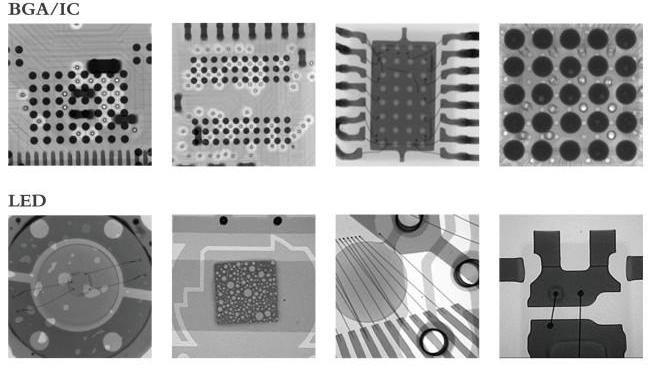
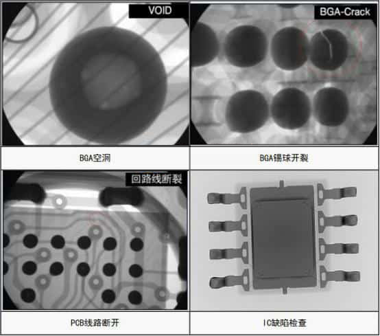
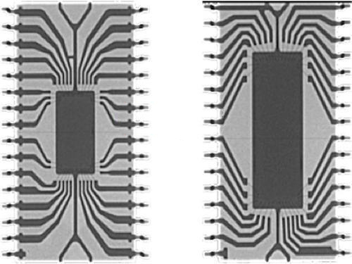
1、IC’s footprint inspection: Peel, cracking, empty, wire bonding.
2、Print circuit boards fabrication inspection: Welding line offset bridging, open circuit.
3、SMT weldability inspection: Solder joints empty inspection and measurement.
4、Circuit line inspection: Open circuit, short circuit, defective or fault connection.
5、 Integrity inspection of solder ball in array package and chip covering packaging.
X-ray inspection devices have seen fast development in recent years; it now has 3D inspection from the previous 2D generation. 2D is transmission x-ray inspection, and it can clear an image of the solder joints and on which single layer PCB. However, it is inadequate for 2 layer reflow soldering PCB because two side solder joints image is overlapped, and difficult to find faults. However, 3D inspection is lamination technology that focused on all layers, and the corresponding image is projected onto a high-speed rotating receiving surface
Since the high-speed rotation of the receiving surface makes the image focal point very clear and the image on the other layers is eliminated. The 3D inspection method can image the solder joints independently on both sides of the plate.
In addition to examining double-sided soldered plates, 3D X-ray can also perform multi-layer image “slicing” inspection of invisible solder joints such as BGA, which is a thorough inspection of the top, middle, and bottom of the BGA solder ball joints.
Simultaneously, this method can also be used to measure through hole (PTH) solder joint, check whether the solder material in the through hole is full, to improve the joint quality of the solder joint significantly. The SPC statistical control function can be connected with the assembly equipment to achieve real-time monitoring of assembly quality
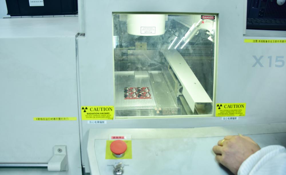
(1) The machine has an X-ray tube that creates X-ray.
(2) The sample is moving on the X-ray machine to inspect each sample position and adjust magnification and inspect the inclination angle.
(3) A device can receive an image that is captured through x-ray.
(1) The inspection effectiveness rate is about 97%, and such defects can be inspected: Cool solder, tin connect, not enough solder, components missing, etc. In particular, an X-Ray can also check BGA, CSP, and other hidden solder joint devices
(2) High test range, X-ray can test inside of the sample.
(3) Short inspection time.
(4) Find defects that cannot be reliably detected by other testing methods, such as cool solder, air holes, and poor forming.
(5) Only need to inspect 2-layer or multi-layer once.
(6) Provide measurement information to evaluate the production process, such as solder paste thickness, solder amount under the solder joint, etc.
For PCB board with higher density, components are smaller, and the ICT test point space is even smaller. In addition to the complex PCB, the test pass rate declined, and the board fault diagnosis and repair costs also increased, which might cause the delivery delay. It will also lose competitiveness in today’s market.
If the X-ray inspection is replaced with ICT, X-ray can guarantee production function and reduce fault diagnosis and repair work. By using X-ray to spot check, SMT production can reduce or even eliminate the batch error. It can measure faults that ICT couldn’t find, such as too little or too much solder, cold sweat, welding, or stoma. These defects are not easily found by ICT functional testing, thus affecting the service life of products.
The X-ray cannot detect the components’ defect, but these things can be tested in the functional test. The X-ray detection should not miss any defects in the manufacturing process and can defects that ICT cannot.
Combined with the above factors, the 3D X-Ray machine can evaluate each solder joint according to its size, shape, and characteristics. 3D X-Ray machines can also automatically detect unacceptable and critical solder joints; otherwise, they would be considered good solder joints in other tests. This can cause premature failure of the product.
There are often circuit board problems in electrical product production and some defects that the eye cannot find. The typical defects of PCB boards are soldering, bonding, and copper foil falling off.
The reason for adhesion: The temperature of the iron should not be too high. The high temperature will make the iron head burn and can not get tin, and easy to fall off the copper foil. The copper foil falls off because the soldering iron should not get too much tin at one time, as too much tin will cause adhesion between the two solder joints.
X-ray can inspect the PCB defects such as cool soldering, adhesion, copper foil falling off.
IC X-ray inspection device mainly uses X-ray to illuminate internal chips. The intense penetration of X-ray can penetrate the chip then create an image. The image will show the chip internal structure fracture situation in a complete view. The main feature of the X-ray is to make sure the chip does not have damage to the chip itself, so this detection method is also called nondestructive flaw detection.
The IC X-ray inspection machine adopts the principle of X-ray transmission to take pictures of the measured object’s internal structure in real-time. Widely used in battery, electronic products processing, casting processing, and other industries, the main product internal defects can be used for practical analysis. Users can easily obtain high-quality, high-magnification, and high-resolution images.
With the development of communication, computer, consumer electronics, and other industries, the future development trend is a smaller ICT space, more invisible welding joints such as BGA, and higher requirements for welding quality. As an emerging process method and analysis,
X-ray detection technology can detect invisible defects under the premise of not destroying the product, reflecting the product’s internal information, and carrying out qualitative and quantitative analysis on the detection results. This is an advantage to find the fault as early as possible and reduce the rejection rate.
Our X-Ray machine has been widely used in PCB surface mount to ensure that we can provide customers with high-quality PCBA products.
C4 Jinxiongdakejiyuan Huanguannan rd, Guanhushequ, Longhua district Shenzhen China
 sales@pcba360.com
 PCBA360
 +86-755-84717796
Certifications

Delivery


<
 Quote
Quote