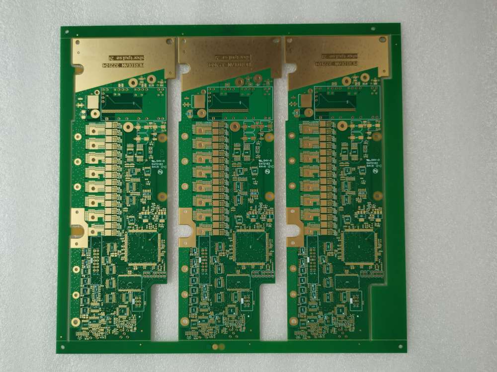
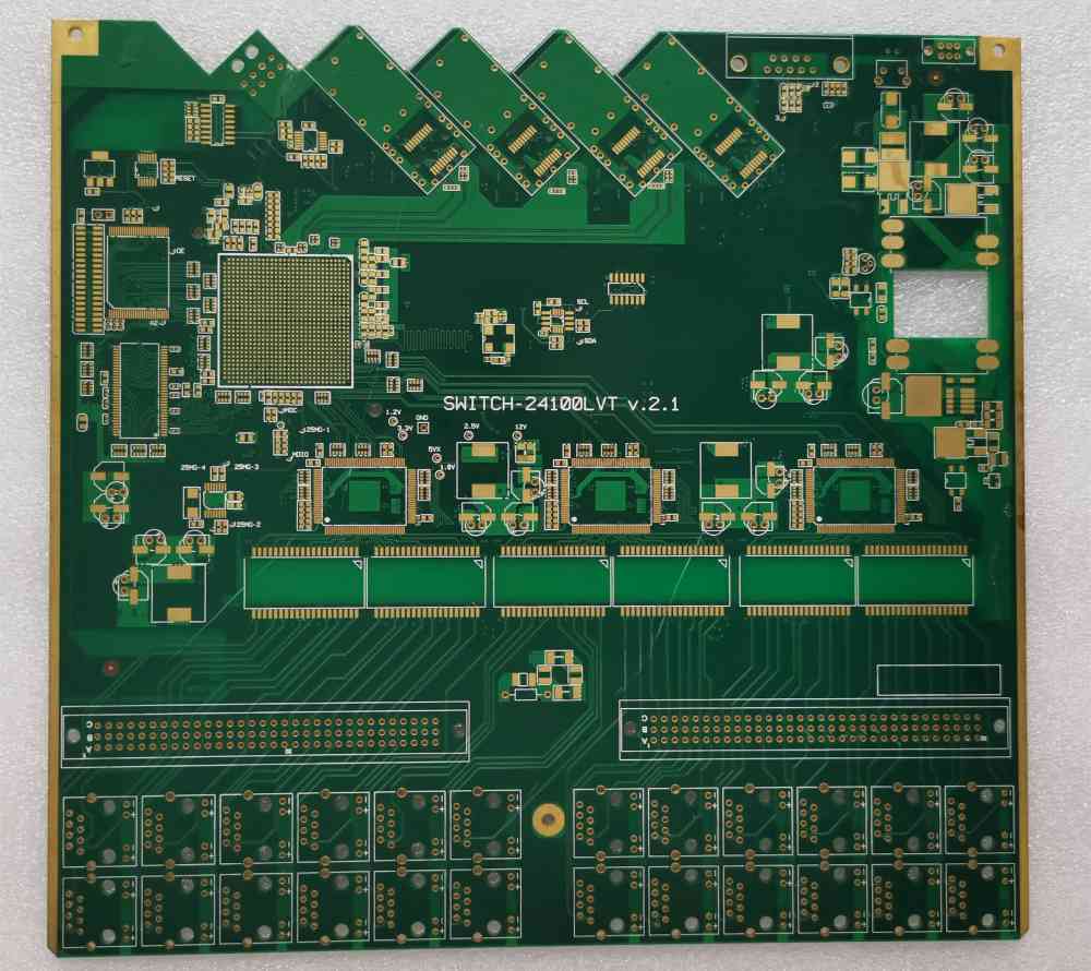
Multilayer PCB or multilayer printed circuit boards are circuit boards composed of two or more conductive layers (copper layers). The copper layer is pressed together by the resin layer (prepreg). Due to the complexity of the multilayer PCB manufacturing process , low production volume, and difficulty in rework, their prices are relatively higher than a single layer and double-sided PCB.
XDF manufacture multilayer PCB up to 56 Layer , accept pure single material or mixed-press
materials
:Fr4, Rogers,Polymide,metal Core . Send Your PCB Files to sales@pcba360.com, We will quote you Very Soon !
Multilayer PCB Manufacturing
Due to the increase in the packaging density of integrated circuits , a high concentration of interconnection lines has resulted, which necessitates the use of multilayer PCB. Unforeseen design problems such as noise, stray capacitance, and crosstalk have appeared in the printed circuit layout. Therefore, the printed circuit board design must minimize the length of signal lines and avoid parallel routes. Obviously, in the PCB single-sided board, even the double-sided board, due to the limited number of crosses circuit that can be achieved, these requirements cannot be satisfied. In the case of a large number of interconnection and crossover requirements, the PCB circuit board must be expanded to more than two layers to achieve satisfactory performance. Thus a multilayer circuit board has appeared. Therefore, the original intention of manufacturing multilayer circuit boards is to provide more freedom in selecting appropriate wiring paths for complex and noise-sensitive electronic circuits.
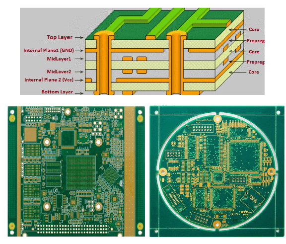
Multilayer PCB circuit boards have at least three conductive layers, two of which are on the outer surface, and the remaining layer is integrated into the insulating board. The electrical connection between them is usually achieved through plated through holes on the cross-section of the circuit board. Unless specified, multilayer printed circuit boards are the same as double-sided boards, generally plated through-hole boards
Advantages:
Multi-layer PCB multiply their density through layering. This increased density allows greater functionality, improving capacity and speed despite the smaller PCB size.
Multilayer PCB increase board surface area through the addition of layers, decreasing overall size. This will allow higher-capacity multilayer PCB to be used in smaller devices, while high-capacity single PCB must be installed into larger products.
Multilayer PCB can accomplish the same amount of work as multiple single-layer board, but does so at a smaller size and with fewer connecting components, reducing weight. This is an essential consideration for smaller electronics where weight is a concern.
Multilayer PCB circuit boards have at least three conductive layers, two of which are on the outer surface, and the remaining layer is integrated into the insulating board. The electrical connection between them is usually achieved through plated through holes on the cross-section of the circuit board. Unless specified, multilayer printed circuit boards are the same as double-sided boards, generally plated through-hole boards
Disadvantages:
Praesent porttitor, nulla vitae posuere iaculis, arcu nisl dignissim dolor, a pretium mi sem ut ipsum. Fusce fermentum.
Praesent porttitor, nulla vitae posuere iaculis, arcu nisl dignissim dolor, a pretium mi sem ut ipsum. Fusce
Praesent porttitor, nulla vitae posuere iaculis, arcu nisl dignissim dolor, a pretium mi sem ut ipsum. Fusce fermentum.
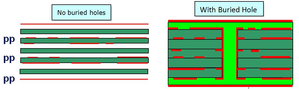
Multilayer printed circuit is the product of electronic technology development in high speed, multi-function, large capacity, and small volume. With the continuous development of electronic technology, especially the extensive and in-depth application of large-scale and very large-scale integrated circuits, multilayer printed circuits are rapidly developing in the following directions: high density, high precision, and high layers, tiny lines and small holes, blind and buried holes, high plate thickness to aperture ratio and other technologies to meet market needs.
1、It can be manufactured in a PCB factory. The four-layer board generally uses a core
with one copper foil on each sideand
a three-layer board with one copper foil on one side. They must be pressed together.
2、The process cost difference between the two is that the four-layer board has one more copper foil and bonding layer.
The
cost difference is not significant. When the PCB factory makes a quote, they are generally quoted on
an even number
basis. Also, 3-4 layers are commonly quoted as a grade. (For example:If you design a 5-layer board, the other party
will
quote at the price of a 6-layer board. That is to say, the price you design for 3 layers is the same
as the price you
design for 4 layers.)
3、In the PCB process technology, the four-layer PCB board is better controlled than the three-layer
board, mainly in terms
of symmetry. The warpage of the four-layer board can be controlled below 0.7% (IPC600 standard), but the size of the
three-layer board is large. At that time, the warpage will exceed this standard, which will affect the reliability
of
the SMT assembly and the entire product. Therefore, the designer shouldnot design the odd-numbered
layer board. Even if
the odd-numbered layer is necessary, it will be designed as a fake even-numbered layer. That is to design 5 layers
into
6 layersand 7 layers into 8 layers.
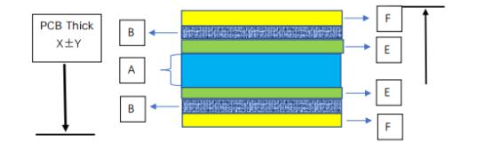
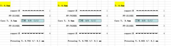
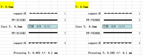
A: Thickness of inner layer B: Thickness of PP sheet
E: Thickness of inner copper foil F: Thickness of outer copper foil
X: Finished board thickness Y: Finished PCB tolerance
1. Calculate the upper and lower limit of pressing:
Usually tin plate: upper limit -6MIL, lower limit-4MIL
Gold plate: upper limit -5MIL, lower limit -3MIL
For example, tin plate: upper limit=X+Y-6MIL lower limit=X-Y-4MIL
Calculate the median = (upper limit + lower limit)/2
≈A+the area of the second layer of copper foil%*E+the area of the third layer of copper foil%*E+B*2+F*2
The inner cutting material of the above conventional four-layer board is 0.4MM smaller than the finished board, using a single 2116 PP sheet to press. For special inner layer copper thickness and outer layer copper thickness that more than 1OZ, the copper thickness should be considered when choosing the inner layer material.
Upper limit = Finished board thickness + Finished on-line tolerance value-[Plating copper thickness, green oil character thickness
(Conventional 0.1MM)]-The theoretically calculated thickness after pressing
Lower limit = finished board thickness-finished product off-line tolerance value-[electroplating
copper thickness, green
oil character thickness
(Regular 0.1MM)]-The theoretically calculated thickness after pressing
|
PP
|
KB
|
KB
|
|---|---|---|
|
1080
|
0.07MM
|
0.065MM
|
|
2116
|
0.11MM
|
0.105MM
|
|
2116
|
0.11MM
|
0.105MM
|
Generally, do not use two PP sheets with high resin content together. If the inner layer of copper is too small,
please
use PP sheets with high resin content. 1080 PP sheets have the highest density and low resin content. Do not press
single sheets as much as possible. Only 2 sheets of 2116 and 7630 PP sheets can be pressed into thick
copper plates above 2OZ. The layer cannot be pressed by a single sheet of PP. 7628 PP sheet can be pressed by a single sheet, 2
sheets, 3 sheets, or up to 4 sheets.
Explanation of theoretical thickness calculation of multilayer PCB board after pressing
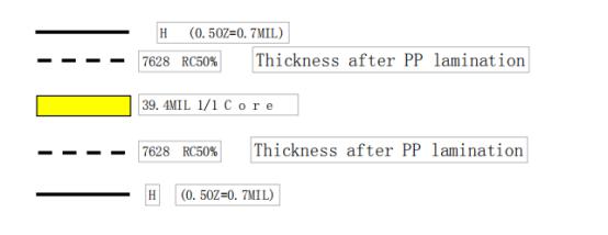
Thickness after PP lamination = 100% residual copper lamination thickness-inner copper thickness*(1-Remaining copper rate%)
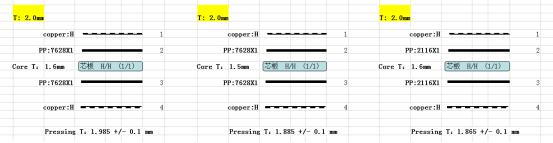
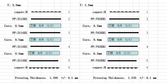
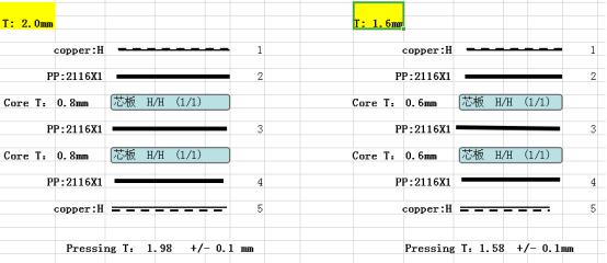
2.0mm 1.6mm 8 Layer PCB Stackup
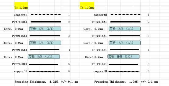
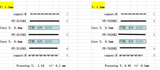
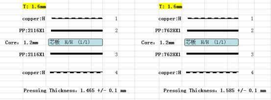
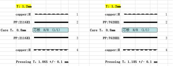
1.2mm 1.0mm 8 Layer PCB Stackup
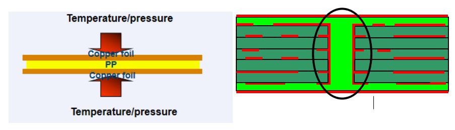
★ Lamination uses high temperature and high pressure to melt the prepreg by heat, make it flow, and turn it into a cured sheet. It is then processing one or more inner etched boards (Black Oxide Treatment) and copper foil into a multilayer board.
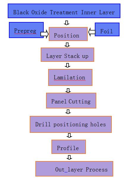
Multilayer PCB Manufacturing Process Steps
Remarks: For 6 layer PCB stack-up and over, two or more inner layers must be pre-positioned so that the holes and circuits of different layers have the correct alignment.
1) Positioning of rivet nails: press the layout of the inner layer board and prepreg with pre-drilled positioning
holes
1、The sequence is set on the template with rivets and then punched with a nail punch
2、Rivets to position
2) Solder joint positioning: set the inner layer board and prepreg with pre-drilled positioning holes according to the layout
1、The sequence is set on the template equipped with positioning pins, and then through the heating several
2、A fixed point, using the prepreg to melt and solidify when heated
We are currently using solder joint positioning-RBM
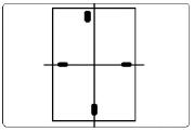
Pre-punched positioning hole for the inner board, the current method we use is as follows: Punch 4 slot holes on the
four sides of the board, two as a group, respectively locating in the X/Y direction, one of which is asymmetrical
design. The purpose is to start to prevent a reaction.
A= 7.112±0.0254MM
B= 4.762 ±0.0254MM
| Thickness | <40mil | 40mil<T<60mil | >60mil |
| temperature | 300℃ | 300℃ | 300℃ |
| Time | 0.3-0.5min | 0.6-0.8min | 0.8-1.0min |
Quality control after RBM-potential problems
1) Interlayer offset: poor RBM positioning or poor heating point condensation, causing
Shift between layers after pressing, after drilling due to
Dislocation of the lines on each layer causes open or short.
Possible reason:
• uInner layer punching deviation
• uThe expansion and contraction of the inner plate is very different
• uRBM staff deflection
• uRBM parameters do not match-the coagulation effect is not acceptable
• uRBM heating head wear-bad condensation effect
• u Lay up personnel put the board improperly, causing the heating point to fall off
2) The inner core is reversed: the order of the inner core is incorrectly placed during RBM, which affects the
quality
of the customer’s assembled board.
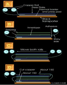
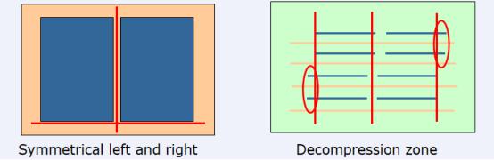
Introduction to Layer Stack-Up Process: The layout process arranges the inner core, prepreg, and copper foil
with
aluminum plates according to the structural requirements and reaches the required height for
pressing. CEDAL layer
stack-up can be divided into four main layouts according to the right picture
A prepreg refers to glass fibers or other fibers impregnated with resin. After partial polymerization, the resin
molecules are slightly cross-linked, which can be softened by heat. However, it cannot be completely melted.
Prepreg specifications
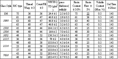
Prepreg specifications
Main Performance characteristics of prepreg
Resin content (R/C)
Resin fluidity (R/F)
Gel time (G/T)
Volatile content (V/C)
Resin content (RC)
1). Resin content definition: the percentage of the weight of resin in the semi-cured to the weight of the
prepreg;
2). Calculation formula: RC=(TW-DW)÷TW ×100%;
RC: Resin content; TW: weight of prepreg; DW: weight of glass cloth after burning.
3) TW can be used as a control indicator when the base weight of the glass cloth is constant
2、Instrument: Electronic balance, accuracy: 0.001 g
3、Sample: 4 “X 4” X 4 pieces
Resin content of prepreg (RC)
• lRC is mainly related to the thickness of the laminate.
• lThe RC is low,and the thickness of the board is thin;
• lIf the deviation of the left, middle,and right of the RC is large, the thickness uniformity of the board will be
poor.
• After controlling the RC of the prepreg, the required thickness can be obtained after pressing, and the Cpk value of the
thickness can be increased.
Comparison table of resin content and PP thickness
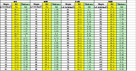
Thickness after PP pressing
1、Thickness = theoretical thickness of single PP-filling loss
2、Filling loss = (1-A side copper residual copper rate) x copper foil thickness + (1-B side copper residual copper
rate) x
copper foil thickness + 0.4*(D2)2*H(inner layer thickness)*N(hole Number)/the whole board area
The relationship between PP film characteristic parameters and resin fluidity:
• The gel time (PG) is large,and the resin has strong fluidity;
• The fluidity (RF) is large, and the resin has strong fluidity;
• The minimum viscosity (MV) is small,and the resin has strong fluidity;
• Large flow window (FW), strong resin fluidity;
When PG is long, RF is high, MV is low, or FW is long, the following situations may occur after pressing:
1、There is a lot of resin flow and poor board thickness uniformity (easy to be thick in the middle and thin on the
edge).
2、White edges appear on the edges of the board due to low resin content.
3、Skateboarding easily occurs.
4、Easy to show texture.
5、The resin content of the board is reduced, which affects the dielectric properties and insulation properties.
Also,anti-CAF performance is poor.
6、The internal stress of the plate is increased, and it is easy to twist and deform after pressing.
When PG is short, RF is low, MV is high, or FW is short, the following situations may occur after
suppression:
1、Dry board, trunk line, dry point.
2、Air bubbles.
3、The cohesive force between core material layers is weakened, and the board is prone to bursting.
4、The peel strength between resin and copper foil is weakened.
• Storage temperature: 21±2℃ or below 5℃
• Storage humidity: below 60%
• Storage time: 90 days and six month
Our current lay up is two types. Controlling the consistency of lay up can ensure uniform force during pressing and avoid white edges due to loss of pressure. This requires the position of the laser beam to be adjusted and fixed when preparing for lay up. Laying the board along with the laser beam in the lay up production.
Controlling the height during lay up can ensure the smooth progress of pressing and achieve maximum productivity.
| Machine | Minimum height | Highest height |
| 48# | 160mm | 170mm |
| 73# | 220mm | 260mm |
• Boards of different sizes cannot lay up together.
• Boards with a difference of more than 15mil in thickness cannot lay up together.
• The boards of different thicknesses are lay up together, the thermocouple must be placed in the middle of the
thin
board, and the ADARA staff shall be notified to increase the curing time by 10 minutes.
• Small plates (less than 10 pieces) of different copper foil thickness can be lay up together by cutting the copper
foil,
and PE release film must be placedbetween the board and the conductive copper foil during production.
• Lay up the board in the middle of the whole cycle.
• Add dummy lay up on the top and bottom of the production board and reach the lowest height.
The Black Oxide Treatmentboard is stored in the environment for a long time, and it is easy to absorb water, causing delamination after pressing
| Process | Storage time |
| B/F | 72hours |
| B/O | 24hours |
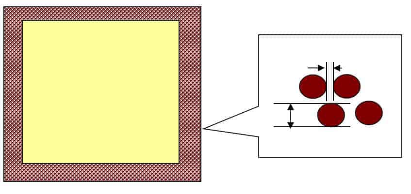
• The edge of the inner board is filled with dummy pads.The pad diameter is required to be 4.0mm, and the spacing is
required to be 1.5mm.
• The two layers of dummy pads corresponding to the inner layer board mustbe staggered by half the pad distance to
balance
the pressure during pressing.
• The dummy pads of adjacent rows should be staggered to improve flow resin.
In the PCB design, if the removed area by the rout is large, a dummy pad is required to be added to the rout area to increase the residual copper rate and reduce the filling. The pad diameter is required to be 4.0mm, and the spacing is required to be 1.5mm.
When designing in array, if the area removed by rout is relatively large, add a dummy pad in the routarea to increase the residual copper rate and reduce the filling. The pad diameter is required to be 1.5mm, and the spacing is 1.0mm.
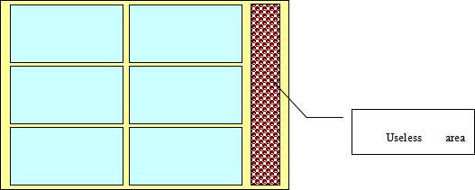
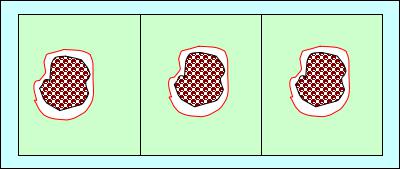
• For designswith broken edges, dummy pads must be filled with a pad diameter of 1.5mm and a spacing of 1.0mm.
• lThe two layers of dummy pads corresponding to the inner layer board are required to be staggered by half the pad
distance to balance the pressure during pressing
2. PP Design Requirements
1、The centrally symmetric structure can avoid the bending phenomenon caused by structural stress.
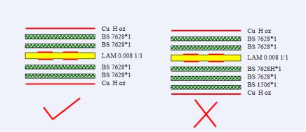
2、High R/C, thin fabric on the outer layer
• The same glass cloth combinationand high resin content are placed on the outer layer.
• Different kinds of glass cloth combinations, based on the principle of symmetry, thin fabrics are placed on the
outer
layer.
3、Warp to warp, weft to weft
The glass cloth yarn contains different yarn counts in warp and weft directions, resulting in different glue content
and
differences in thermal expansion in the two directions.
4、Each layer of prepreg has a reasonable thickness
• The thickness andglue content is high. The thickness is not suitable for control
• Small thickness, low glue content,and low adhesion
5、Minimum number of layers
• Many layers, high cost, andnot suitable for process control
Pressing Method – Hydraulic Press
The structure of the hydraulic pressing machine is vacuum type and standard pressure type. The plate between the
openings of each layer is clamped between the upper and lower hot plates. The pressure is from bottom to top, and
the
heat is transferred from both upper and lower hot plates to the plate.
Advantages: simple equipment, low cost, large output.
Disadvantages: large amount of glue flow, poor thickness uniformity.
The Cedal is a revolutionary laminating machine. Its operating principle uses continuous coiled copper foil that laminates in a closed vacuum chamber. Current is then applied at both ends. Due to its resistance, the copper foil generates high temperature and heats prepreg, and the pressure is applied by the upper air bag to achieve the compression effect.
Advantages:
• Using the upper and lower interlayer copper foils for electric heating, energy-saving,and low operating cost.
• Small temperature difference between the inner and outer layers, uniform heating, good product quality.
• Cycle time is short, about 60minutes.
• Fast heating rate (35/min).
• Disadvantages:
• The equipment has a complex structure and high cost.
• Single machine output is small.
• The pressure is a pneumatic working method, which cannot provide high pressure.
It can help to remove gases, air, and small monomer residues generated by solvent volatilization.
The curing agent DICY is very stable at room temperature and can be cured quickly after the temperature rises.
Experiments show that 170°C is the ideal curing temperature. Therefore, it is necessary to control the temperature
above
170°C during the pressing process to complete the curing reaction.
Maintaining a specific heating rate can appropriately increase the resin’s fluidity, thus improving the resin’s
wettability and preventing problems caused by thermal stress.
Pressure:
Offset the vapor pressure generated by volatiles. Improve resin fluidity. Increase interlayer adhesion. Prevent
deformation due to thermal stress during cooling
• Use a thickness gauge to measure the thickness of the four corners and a midpoint of each plate
• The test point is 50 mm from the edge of the board
• Thickness tolerance: general thickness requirements ± 10%
• Use a thickness gauge to measure the thickness of the four corners and a midpoint of each plate
• The test point is 50 mm from the edge of the board
• Thickness tolerance: general thickness requirements ± 10%
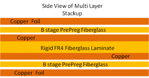
Multilayer PCB is manufactured by stacking two or more circuits on top of each other, and they have reliable pre-set interconnections. Since drilling and plating have been completed before all layers are pressed together, this technique violates the traditional manufacturing process from the beginning. The two innermost layers are composed of traditional double panels, while the outer layers are different. They are composed of single independent panels. Before pressing, the inner substrate will be drilled, through-hole plated, pattern transferred, developed, and etched. The outer layer to be drilled is the signal layer, which is plated through so that a balanced copper ring is formed on the inner edge of the through-hole. The layers are then rolled together to form a multilayer PCB, which can be connected to each other (between components) using wave soldering.
Pressing may be done in a hydraulic press or an overpressure chamber (autoclave). In the hydraulic press, the
prepared
material (for pressure stacking) is placed under the cold or preheated pressure (high glass
transition temperature
material is placed at a temperature of 170-180°C). The glass transition temperature is the temperature at which an
amorphous polymer (resin) or part of the amorphous region of a crystalline polymer changes from a hard and brittle
state
to a viscous, rubbery state.
It is a container filled with high-temperature saturated water vapor, and high-pressure can be applied. The laminated substrate (laminates) sample can be placed in it for a period of time to force moisture into the board, and then take out the sample again. Place it on the surface of high-temperature molten tin and measure its “delamination resistance” characteristics. This word is also synonymous with the pressure cooker, which is commonly used by the industry. In addition, in the multilayer board pressing process, there is a “cabin press method” with high temperature and high-pressure
It refers to the traditional lamination method of early multilayer PCB boards. At that time, the “outer layer” of MLB was mostly laminated and laminated with a single-sided copper thin substrate. It was not used until the end of 1984 when the output of MLB significantly increased. The current method is the copper-skin type large or mass pressing method (Mss Lam). This early MLB pressing method using a single-sided copper thin substrate is called cap lamination.
The multilayer board pressing often refers to the wrinkles that occur when the copper skin is improperly handled. Such shortcomings are more likely to occur when thin copper skins are below 0.5 oz and laminated in multiple layers.
It refers to the gentle and uniform sag on the copper surface, which may be caused by the partial protrusion of the steel plate used in pressing. If it shows a neat drop of the faulty edge, it is called “dish down.” If these shortcomings are left on the line after copper
When the multilayer board is pressed, in each opening of the press, there are often many “books” of bulk materials (such as 8-10 sets) of the board to be pressed. Each set of “bulk materials” (Opening) Book) must be separated by a flat, smooth, and hardened stainless steel plate. The mirror stainless steel plate used for this separation is called “caul plate” or “separate plate.” At present, AISI 430 or AISI 630 are commonly used.
Refers to the mass-produced multilayer board, the outer layer of copper foil and film are directly pressed with the inner skin, which becomes the mass lam of the multilayer board. This replaces the early traditional single-sided thin substrate Press legal.
When multilayer boards or substrate boards are laminated, kraft paper is often used as a heat transfer buffer. It is placed between the hot plate (Platern) of the laminator and the steel plate to ease the temperature rise curve closest to the bulk material. Between multiple substrates or multilayer boards to be pressed. Try to minimize the temperature difference of each layer of the sheet; the commonly used specifications are 90 to 150 pounds. Because the fiber in the paper has been crushed after high temperature and high pressure, it is no longer tough and difficult to function, so it must be replaced with a new one. This kind of kraft paper is co-cooked with a mixture of pinewood and various strong alkalis. After the volatiles escape and the acid is removed, it is washed and precipitated. After it becomes pulp, it can be pressed again to become rough and cheap paper material.
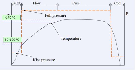
When the multilayer board is pressed and the plates are placed and positioned, they will start to heat and be lifted by the hottest layer from the bottom. Afterward, lift with a powerful hydraulic jack (ram) to press each opening (bulk materials in the opening) and are bonded together. At this time, the combined film (prepreg) begins to gradually soften or even flow, so the pressure used for the top extrusion cannot be too large. This is to avoid slippage of the sheet or excessive flow of the glue. This lower pressure (15-50 PSI) initially used is called “kiss pressure.” However, when the resin in the bulk materials of each film is heated to soften and gel and is about to harden. It is necessary to increase to the full pressure (300-500 PSI) so that the bulk materials are tightly combined to form a strong multilayer board.
Before pressing multilayer circuit boards or substrates, various bulk materials such as inner layer boards, films and copper sheets, steel plates, kraft paper pads, etc., need to be aligned, aligned, or registered up and down to prepare. Then it can be carefully fed into the pressing machine for hot pressing. This kind of preparatory work is called Lay Up. To improve the quality of multilayer boards, not only this kind of “stacking” work must be carried out in a clean room with temperature and humidity control, but also for the speed and quality of mass production. Generally, the large-scale press method (Mass Lam) in construction, even “automated” overlapping methods are needed to reduce human error. To save workshops and shared equipment, most factories combine “stacking” and “folding boards” into a comprehensive processing unit, so automation engineering is quite complicated.
Before pressing multilayer circuit boards or substrates, various bulk materials such as inner layer boards, films and copper sheets, steel plates, kraft paper pads, etc., need to be aligned, aligned, or registered up and down to prepare. Then it can be carefully fed into the pressing machine for hot pressing. This kind of preparatory work is called Lay Up. To improve the quality of multilayer boards, not only this kind of “stacking” work must be carried out in a clean room with temperature and humidity control, but also for the speed and quality of mass production. Generally, the large-scale press method (Mass Lam) in construction, even “automated” overlapping methods are needed to reduce human error. To save workshops and shared equipment, most factories combine “stacking” and “folding boards” into a comprehensive processing unit, so automation engineering is quite complicated.
You probably want to widen your knowledge about multilayer PCB. This is one good reason why you have visited this page. Also, you may wish to import multilayer Printed Circuit Boards. Whatever the case may be, our guide will offers the best solution for all your PCB needs.
What does Multilayer PCB Mean?
Multilayer PCB can be referred to as a multi layer circuit board that is composed of three or more layers. This is made up of a substrate layer, which features a conductive metal on its two sides. It also offers enhanced functionality. They are utilized in complex devices that require a very high number of connections.
Multilayer Printed Circuit Boards must feature at least three layers of conductive layers, which are located at the
center of the material. This multilayer PCB manufacturing entails the fusing of fiber-glass alternating
epoxy-infused
conductive core materials and layers.
Both of them are laminated using high hydraulic press pressure and temperature. This process leads to the prepreg
melting, which later results to the joining of these layers.
Steps Used in the Manufacturing of Multilayer PCB
The manufacturing process of multilayer circuits involves some steps. Let us consider them.
Developing the Desired Design
Plan the layout PCB design following all the requirements and encode it. By doing this, you are making sure that the
different aspects and parts of the designs are error-free. A completed PCB design is then ready for fabrication
building.
Printing of the PCB Design
As soon as the check completion has been finalized on the design, then it can be printed. You punch the registration
hole to serve as a guide for aligning the films as you continue with the process.
Print the Copper Utilized for the Interior Layer
This step is the first while making the inner layer of the PCB. You print the multilayer PCB design; then copper is
re-bonded to the lamine piece that serves as the PCB structure.
Discard unwanted copper
Copper that photoresist does not cover is removed with a strong and effective chemical. As soon as it is removed, it
leaves just the needed copper for your PCB.
Lamination of the PCB Layers
Once the layers are free from defects, then you can fuse them. You can achieve this process in two spes, which
include
the lay-up and the laminating step.
Drilling
Before you drill, the drill spot is located with an x-ray machine. This helps in securing the PCB
stack.
PCB Plating
This process helps in fusing the different PCB layers making use of a chemical.
Imaging and Plating of the Outer Layer
By doing this you are guarding the copper found on the outer layer by applying the photoresist.
Final Etching
Applying Solder Mask
Completing Silk-screening and PCBs
PCB plating is done to make sure that the soldering of the components can be achieved. The process of
screening points
all the important information on the PCB.
Electrical and Testing Reliability
To ensure functionality, the technician carries out tests on several areas of the PCB.
Profiling and Cutting
According to the requirements of the customer, different PCBs are cut from the initial panel. Then the inspection of
the
board is done, and the errors rectified before it is sent for delivery.
Materials Used in the Manufacturing of Multilayer PCB
The different materials utilized in manufacturing multilayer PCBs are boards, copper foil, resin system, substrate, vias, infused fiberglass sheet. Using an alternating sandwich, you can laminate these materials together.
All the planes of copper are etched and the plating through of all internal vias is done before the layers.
Multilayer PCB: Benefits
Multilayer PCBs come with lots of great benefits. Some of them include:
• Higher assembly density
• Provision of high speed and high capacity, as a result of their electrical properties
• Weight reduction of devices
• Elimination of connectors needed for multiple separate PCBs, thereby simplifying its construction.
Multilayer PCB: Uses
Multilayer PCBs can be utilizes in many areas. Let’s consider some of them.
• They are used in manufacturing CAT scan, heart monitors, and modern x-ray equipment.
• Utilized in the production of high-speed circuits due to their functionality and durability
• Used for headlight switches and onboard computers due to their high functionality and heat resistant ability
• The running of machinery and industrial control system utilize them due to their small size and
durability.
• Consumer electronics such as microwaves and smartphones also make use of multilayer
PCBs as a result of their small size
and functionality.
• Satellite applications, GPS, and signal information, also make use of multilayer PCBs
• Used in the production of computer electronics that are utilized in motherboard servers due to its
performance and
space-saving attributes.
Identifying a Multilayer PCB
You can identify a multilayer PCB through the following
• How your electronic equipment operates briskly, as well as the ultimate board’s operational
setting
C4 Jinxiongdakejiyuan Huanguannan rd, Guanhushequ, Longhua district Shenzhen China
 sales@pcba360.com
 PCBA360
 +86-755-84717796
Certifications

Delivery


<

 Quote
Quote