High Quality Laser Cut
PCB Stencil for SMT Use

We can provide you with our quality Basic Stencil and framework so you can handle
assembly from the convenience of your own worktable.

Never Ignore the Importance of SMT Stencil

Introduction to SMT Stencils

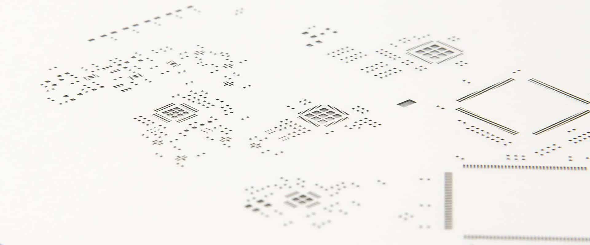
A surface mount technology (SMT) stencil may also be called a PCB stentcil, solder paste stencil, or laser stencil. An SMT Stencil’s main purpose is to simply transfer the solder paste to a bare circuit board. A stainless steel foil is laser cut to create an opening for each surface mount device on the board. Once the PCB stencil is properly aligned with the top of the board, the solder paste is applied over the openings (in a single pass, with a metal squeegee). When the stainless steel foil detaches from the board,  solder paste remains, ready for the manufacture of the surface-mount device (SMD). In contrast to manual soldering procedures, this process ensures consistency and saves time.


laser cut stencils

The deposited solder paste released to the board is manipulated by opening the size of the aperture, and the thickness of the SMT stencil is made out of stainless steel. Excessive paste will cause problems for connectivity and bridging, whereas less paste will compromise the strength of the soldering and joints.


The thickness of an SMT stencil varies with the device for which it is being used. 0.020” pitch small outline integrated circuits (SOICs) can work better with a stencil giving a thin solder paste, whereas thick solder paste works best with 0.050” pitch SOICs. The thickness of the paste stencil for solder ranges from 0.001” to 0.003”. The normal thickness for most of the PCB boards is generally between 0.004” and 0.007”.


Selective Sizes with laser cut stencils Are Now Offered with Nano Coating


For nano coating, the contacting sides of the tiny components are applied with a water-resistant nano coating that opposes solder and flux as well. This phenomenon results in the better release of solder stencil for the tiniest components. The application is made in the factory so the component is ready to use at the time of purchase. The nano coating is  recommended for fine pitches of QFN and IC, micro ball grid arrays (BGAs), and the electronic components of 0201 type.


The 6 most common varieties of PCB stencils, by size and type, are outlined below.

1. PCB stencil


▶ Size: 10” x 12” max


▶ Type: Squeegee


▶  Add on: Board holder


2. Prototype Oversized Stencil (SMT)


▶ Size: Over 10” x 12”


▶ Type: Squeegee


▶ Add on: Board holder


3. Kit-Leaded Prototype SMT Stencil


▶ Size: 10” x 12” max


▶ Type: Solder leaded paste


▶ Add on: alcohol wipes x2, gloves x1 pair, temperature marker


4. Kit-Leaded Prototype PCB Stencils Oversized (SMT)


▶ Size: Over 10” x 12”


▶ Type: Solder leaded paste


▶ Add ons: alcohol wipes x2, gloves x1 pair, temperature marker


5. Prototype Kit-Lead Free SMT Stencil


▶ Size: 10” x 12” max


▶ Type: Solder lead-free paste


▶ Add ons: alcohol wipes x2, gloves x1 pair, temperature marker, grab and place tool


6. Prototype Kit-Lead Free Stencil Oversized (SMT)


▶ Size: Over 10” x 12”


▶ Type: Solder lead-free paste


▶ Add ons: alcohol wipes x2, gloves x1 pair, temperature marker, grab and place tool


Where Can PCB Stencils Be Made?
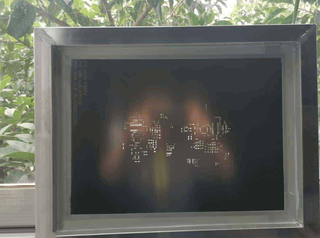
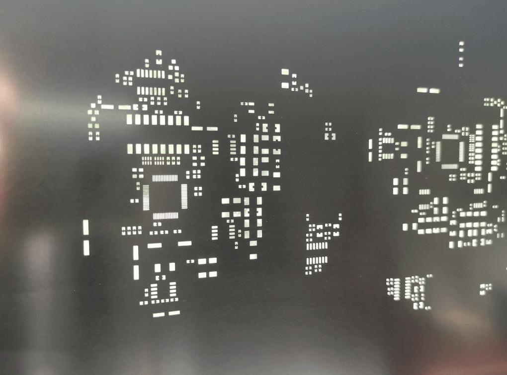

framed stencils

Framed stencils manufactured by PCB stencils unlimited are easy to obtain. Upload your Cream Top from the desired PCB layout software after exporting it. After automatic calculation for the best suitable thickness of your stencil, send the stencil file to sales@pcba360.com;you will get a quote immediately .


If your PCB fabrication house can make stencils, they can also make stencils for you. A Gerber file is important for panel making. Don’t forget to ask them to make the GBC file if you want to make PCB stencil yourself!


IPC 7525 has a detailed document about calculations of smt stencil thicknesses. The approximate value shall be 2.64 + 0.0831 * pitch-of-component.


PCBs revolutionized the electronics industry when they replaced the earlier method of circuit design on a chassis. Before PCBs, electronic circuit design involved bulky and loose components, such as connector lugs and screw terminals, which resulted in end products with large footprints and higher costs. By replacing manual point-to-point wiring, PCBs not only automated the process of circuit design but also greatly reduced the size of electronic end products.


Since the advent of PCBs in the beginning of the 20th century, it has gone through an evolutionary process of design improvements—such as  transitioning from single-layer designs to 20+ layer boards. Overall, the PCB design process can be broken down into the following key steps:


Electrical design

Physical design

Manufacturing

The manufacturing process is followed by the placement of components on the PCB called ‘board assembly’. Traditionally, the assembly process consists of following steps:


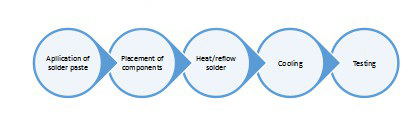
The Assembly Process with SMT Stencil

Conventionally, the board assembly process was performed manually placing and soldering the electronic components by hand. However, with the increasing complexity of circuit boards and extremely small sizes of surface mount packages, board assembly is moving towards application of solder paste using PCB stencils and machine-based component placement.


During the PCB assembly process, stencil solder paste only needs to go where a component must be in electrically conductive contact with a metal landing pad on the board itself. The hand soldering method only makes sense where the design is simple, and the number of components is minimal. Naturally, hand soldering techniques are also prone to human error, which results in inconsistent results.


On the other hand, PCB stencils resolve these issues and are an effective and efficient method of applying solder paste. A stencil, as the name suggests, is a tool to make repetitive impressions. A PCB stencil acts as a guided template for the application of solder paste only on the desired areas of the board. The smt stencil is placed on the circuit board and aligned in the correct position. A runner is moved across the laser cut stencil screen which squeezes the appropriate amount of stencil solder paste through the holes onto the circuit board.


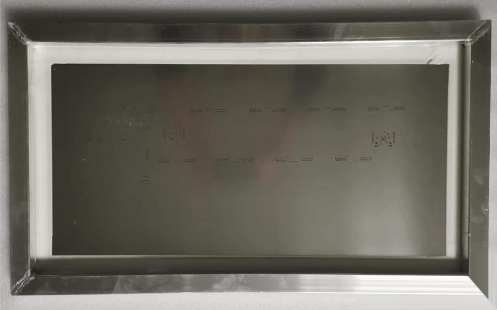
Every PCB stencil is customized according to the design of the PCB so that the solder paste gets applied only on the solder pads. For surface mount technology, the pcb stencils are called SMT stencils. An SMT stencil consists of an outer aluminum frame, polyester mesh, and stencil foil. Stencil foil is tensioned and fixed to the aluminum frame by a polyester mesh.


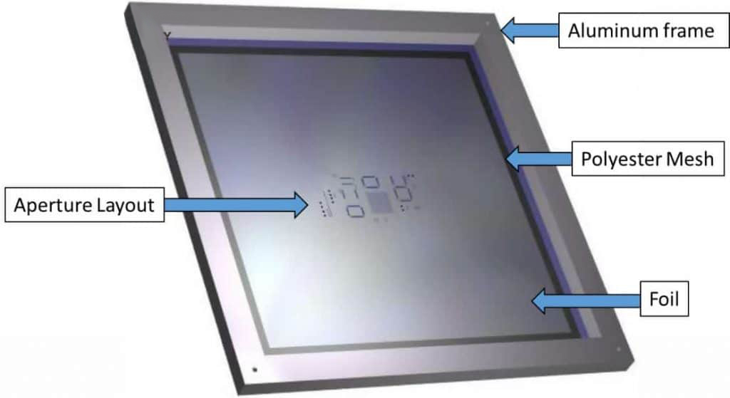
Stencil foil stretched and held to a frame by polyester mesh.

How do you make a PCB Stencil ?

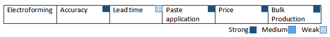
Typically, PCB stencils are made of stainless steel or nickel and can be categorized based on the manufacturing process (process by which aperture is formed on the solder stencil foil), which follows.


Electroforming: This is an additive process by which stencil foil is created by electroforming nickel.  This process is also known as E-FAB. Although this process results in a higher initial cost,price is independent from the number of apertures. Finally, higher processing time is considered a drawback of this manufacturing process.
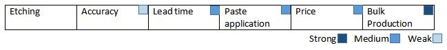

Chemical Etching:


This is a subtractive process by which apertures are achieved through chemical etching. This is relatively a low-cost process; however, it results in inferior results due to rough aperture sidewalls.


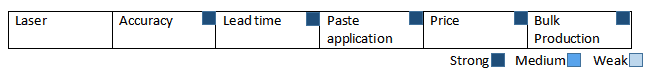
What is Laser cut stencils :


This is also a subtractive process by which removal of the laser cut stencil foil material is achieved by laser cutting. Naturally, laser cutting  results in finer results and helps in achieving greater accuracy. Laser cutting also produces more consistent results than the chemical etching process. Since the process is not dependent on the chemical conditions, there is essentially no requirement for protection from moisture.


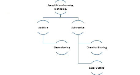
Types of stencil manufacturing technologies.

Depending on the method chosen for the application of solder paste, stencils can be further divided into following types:


Framed Stencils


These laser-cut solder paste stencils are permanently mounted on the frame where the border mesh provides the necessary tension to the stencil foil. These are designed for bulk machinery production.


Frameless Stencils


These stencils are not required to be permanently mounted on the outer frame. These low-cost stencils are recommended for prototype PCB assembly or short runs.


Prototype PCB Stencils

Prototype pcb stencils are designed for manual printing application. It removes the element of human error from the manual printing process.


Other Important Information


How to Generate a smt Stencil file from a PCB File


Generate a Gerber file from the PCB, and then send the Gerber file to the stencil manufacturer to make the stencil.


Generating a PCB Gerber file:


➤ Open the PCB file:open all layers in setup, then click view to confirm and save.


➤ Create a subdirectory: click on the file, use the drop-down arrow to select create in the pop-up dialog box CAM,andtype in the folder name, then click OK.


➤ Output Gerber file: Click Addand a dialog box pops up, fill in the drawing document name in the file name, use the drop-down menu to select the drawing type in the document field, and select the corresponding defined layer name in the pop-up dialog box. Define the output layer and the content of each layer at the level, click OK, then click Run.


➤ Output D code file: open the file and select the Gerber connection diagram at the top or bottom of the dialog box. The default values of each item in the dialog box pop up, thenclick OK.


➤ Output list file: Put all Gerber file lists into a folder, compress them into a compressed package, and save.


PCB Stencil Design Tips


Circuit Board Stencil

Whether to get perfect and reliable solder joints, printing your stencil design is the key first step. The opening size of the surrounding pad stencil is directly related to the thickness of the stencil. Generally, thicker stencils can be designed with an opening slightly smaller than the pad size, while the opening size of the thinner stencil can be designed1:1. It is recommended to use a laser to make a steel mesh with openings and electropolishing.


◆ PCB Stencils design of surrounding pads


The thickness of the stencil determines the amount of solder paste printed on the PCB. Too much solder paste will cause bridging during reflow soldering. Therefore, it is recommended that the 0.5mm pitch QFN package use a 0.12mm thick steel mesh, and the 0.65mm pitch QFN package use a 0.15mm thick steel mesh. The size of the stencil opening can be appropriately smaller than that of the pad to reduce the occurrence of solder bridging.


◆ PCB Stencil design of heat dissipation pad


When the exposed pads on the bottom of the chip are soldered to the thermal pads on the PCB, the gas in the thermal vias and large-size pads will overflow outwards, resulting in certain air holes. Therefore, if the solder paste area is too large, it will produce various defects (such as sputtering and solder balls, etc.). However, it is almost impossible to eliminate these pores;it is possible only to minimize the pores. When designing the stencil in the thermal pad area,careful consideration is needed.


It is recommended to create multiple small openings in this area instead of one large opening. The typical value is 50% to 80% solder paste coverage. Practice has proved that the solder joint thickness of 50μm is very helpful to improve board-level reliability. In order to achieve this thickness, it is recommended that the solder paste thickness for the underfill thermal via design beat least 50%; for the through hole, the coverage rate is at least 75% the above.


How to clean an SMT Stencil


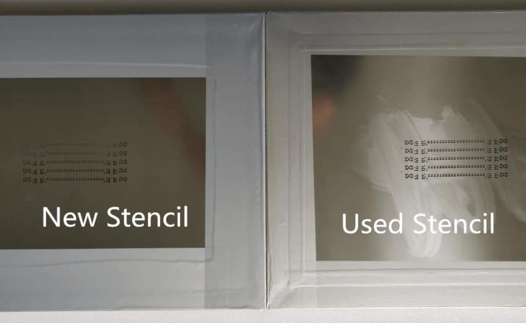
Stencil Solder Paste

SMT stencils are generally cleaned with professional cleaning equipment. Presently, the mainstream of the market is the smart stencil cleaning machine, which is aimed at the electronic industry SMT stencil, copper stencil, wire stencil, microporous stencil, and wafer trays. For the cleaning of similar stencils, the equipment uses compressed air as energy, does not require electricity, and is not a fire hazard.


It adopts a human design and one-button operation, which helps complete cleaning and drying tasks; it utilizes high performance automatic operation of air pressure. As for cleaning equipment, the cleaning fluid is recycled, with low loss. click to know more about how to clean smt stenicl .


SMT Stencil Manufacturers List:

China and India have a strong base of SMT stencil manufacturers. Here is a list of few suppliers based in different regions around the globe:

Region Country Company
APAC China XDF PCB
APAC Australia MasterCut
APAC China Found Printed circuit Board Co.
APAC China MorePCB
APAC China PCB Sino
APAC China JLC PCB
APAC China PCB Way
APAC China ALL PCB
APAC India Satchitanand Group
APAC India Asahitec
APAC India Stencil Point
APAC India Kristeel-shinwa
Europe Germany LPKF
Europe Germany Becktronic
Europe Germany Koenon
Europe Italy ALBA PCB
North America US Tropical Stencils
North America US Stencils Unlimited
North America US EPEC Engineering
North America US OSH Stencils


Top 10 PCB Stencil Factory in Europe

Are you looking for the best PCB stencil manufacturer in Europe? There are lots of them. With 44 countries in the continent, rest assured that you can find or more PCB stencils factories to handle your circuit board project in Europe.

The challenge, however, is how to find out the best pcb stencils manufacturers. With lots of them, you may be confused about the factory that offers the best service.

Also, you want to consider other important factors, such as the type of PCB  stencil service the factory offers, the cost of their service, and the turnaround time.

You can be confident now knowing that you are reading a guide that will walk you through the entire process.

This article is about the 10 leading SMT stencil factories in Europe. It is also about some of the reasons why we selected the manufacturers on the list.

What is SMT Stencil?

Let us understand what an SMT stencils means before we proceed to show you some of the smt stencilsprinters you can find in any of the European countries.

An SMT stencil is known by many other names. It can be called Laser cut Stencil, PCB Stencil, or Solder Paste Stencil. We are pointing this out so you don’t become confused when you come across how we interchanged the names in the course of reading this guide.

An SMT Stencil is the process of transferring the solder paste to a Printed Circuit Board (PCB). This is done because the process of designing circuit boards (PCBs) can be a bit complicated.

So, it is pertinent to ensure that the solder paste required for modeling the board the way it should be is done the right way. That is what the smt stencils is used for.

Worthy of mention is that the smt stencils process is mostly used when using the Surface Mount Technology (SMT) to design Printed Circuit Boards (PCBs).

Besides, the mounting or placement of the Surface Mount Device (SMD) needs to be accurate. For this to go on as expected, a stainless-steel foil would be laser cut. The aim of doing this is to create an opening on the circuit board. This way, it would be easier to mount or place the Surface Mount Device (SMD) on the Printed Circuit Board (PCB).

The 10 Best PCB Stencils Factories in Europe

Here is the subject of this guide – the top European PCB manufacturers that specialize in PCB stencilS .

We selected these factories or PCB manufacturing companies based on many criteria, including the years of experience, the quality of their pcb stencils service, and the overall customer satisfaction.

You can, therefore, be confident that you would get the best pcb stencils service and value for your money.

When you have a smt stencils printing project, these are some of the best factories to contact in Europe:

1. PHOTOCAD

Some top European PCB manufacturers offer a wide range of circuit board design services, including smt stencils .

However, others focus on just smt stencil . For this type of circuit board factories or manufacturers, their goal is to provide an all-around smt stencil service.

One of such manufacturers is PHOTOCAD. It is a German step stencil SMT manufacturer that takes orders for different kinds of SMT stencils products.

It is imperative to mention here that PHOTOCAD has an eye for details. And as their slogan suggests, they ensure that “precision works” in all of the laser cut stencils solutions they offer.

Services

The company also offers a variety of step smt stencil design services that are targeted at different kinds of customers.

For example, there is an option for manufacturing SMT stencils that are optimized for the smallest components.

Likewise, the factory offers a Basic Plan service that has to do with the production of laser cut stencils by using standard applications.

SMT Stencil Technology

The process of manufacturing the SMT stencil is also commendable. The manufacturer uses high-precision smt stencils technology as a way of ensuring that the pcb stencil printing process step by step is achieved.

The company also delivers optimum results for circuit board assembly and solder paste printing. This is done by offering additional surface finishing solutions for the stencil circuit boards. The common solutions used here are electropolishing and nano-cutting.

By and large, you would love to hire PHOTOCAD to handle your step stencil SMT printing because of the excellent service the factory offers.

Some of the other reasons why you want to partner with them are:

  • Providing a wide range of storage systems and solutions
  • Optimal configuration for your stencil SMT
  • The use of standard and more sophisticated SMT stencil technology
  • Individualized SMT stencil solutions
  • Affordable step stencil design

2. Becktronic

Germany has one of the largest concentrations of PCB stencil printer factories. So, if you are looking for where to get the service cheaper and ready in the shortest time possible; go to Germany.

We have yet another largest PCB manufacturers in Germany. The name of this manufacturer is Becktronic and it is your one-stop provider of full-scale SMT stencil services.

Becktronic offers an optimized or personalized stencil printing service. This way, you can get the best out of your solder stencil.

This is not leaving out the fact that this PCB manufacturing Europe service provider is also committed to offering you the best service. This is why you can be sure of getting other options, such as choosing to optimize your stencil printing based on a wide range of grid dimensions and templates.

Individual SMD Stencils

Going for the individual SMD stencils option is one of the best ways to get the best out of your stencil printing.

Becktronic offers this stencil SMT service because it understands how important it is in terms of being a basis for precise solder paste printing.

The individual SMD stencils solutions offered by the company are not only competent and reliable as it pertains to your requirements for the printing. The other impressive factor is that the manufacturer (Becktronic) takes charge of most of the processes, starting from the optimal execution of the SMD stencil to the assurances of consistency in the quality control process.

In addition to all that, Becktronic also offers professional or personal advice. This is done to help you and the other customers to find and choose the right SMT stencil solutions.


3. Quick-teck

Quick-teck is a PCB stencil factory located in Hertfordshire. The company prides itself to be the “Low-Cost UK Circuit Board Manufacturer.”

But that is not the main value that the company delivers. The main value is that asides from the PCB design services, the factory also accommodates pcb stencils . This way, it offers a broad range of SMT stencil services that are targeted to cater to the needs of different kinds of customers.

The Laser Stencil is the most common stencil printing that it offers. For this, the laser cut stencils are made of stainless steel and would be cut for printing the solder pastes.

The customers are also allowed to select either the stencil sheet or the framed stencils. The one they selected would then be shipped together with the Printed Circuit Boards (PCBs).

Several specifications are applied to the laser stencil solutions offered by Quick-teck. Some of these specifications include:

  • The use of laser technology
  • Hardened special steel material is used for the design
  • The SMT stencil would be subjected to a surface finishing before it would be shipped
  • Four fiducials at each corner
  • You can also get free shipping

Why Should You Choose Quick-teck for Your PCB Stencil Solutions?

Thousands of customers have patronized this stencil printing factory in Europe. A majority of those customers are satisfied with the services they got. We are sure you will feel the same way after letting Quick-teck handle your laser stencil.

Here are some of the reasons why you should consider working with them:

  • The factory safeguards your intellectual property by providing a Non-Disclosure Agreement (NDA).
  • The factory can take minimum orders, as low as 1 low-cost RoHS Compliant PCB prototype.
  • They also offer on-time delivery. Ideally, they offer a standard lead-time of 9 working days maximum for low production orders and up to 5 weeks for large volumes.


4. Multi-Circuit-Boards

The quality of the Multi-Circuit-Boards services in the circuit board market is not in doubt. As much as the factory is diversified, it still has considerable control and a mastery of the different kinds of PCB designs and production processes. The stencil SMT process is also inclusive.

As the name of the manufacturer signifies, it focuses on the provision of services across multiple Printed Circuit Board (PCB) markets. It doesn’t matter if you are looking for PCB design or circuit board prototypes. It does not also matter if you are looking for SMD stencils or toroidal transformers.

Whatever it is you are looking for, rest assured that Multi-Circuit-Boards has got you covered. Since we are looking for PCB stencil printer services, let us see how the factory can help us out.

SMD Stencils

This is one of the stencil SMT services that Multi-Circuit-Boards offers. The solder pastes and adhesive stencils (laser cut stencils) are one of the most important requirements for any Surface Mount Technology (SMT) to be successfully used to place Surface Mount Components (SMD) on a circuit board.

One of the unique attributes of the SMD Stencils from Multi-Circuit-Boards is that it is usually manufactured using laser technology. The use of this technology is the reason why the PCB Stencils solutions from Multi-Circuit-Boards have higher precision and maintain consistent quality.

Multi-Circuit-Boards also offers several other services that make it one of the top European PCB manufacturers. These services include but are not limited to:

  • Deburring/double-sided brushing
  • Unlimited pads
  • Final treatment, such as nano protection and electropolish
  • Up to 8 fiducial marks
  • Edge protection
  • Pad manipulation


5. NewburyElectronics

NewburyElectronics is your one-stop PCB manufacturing company that offers a one-stop Electronics Contract Manufacturing (ECM). This means that you wouldn’t necessarily need to look for additional ECM services elsewhere because everything is offered in-house by NewburyElectronics.

The factory also offers unparalleled Surface Mount Technology (SMT) Assembly services. These SMT services are offered for a wide variety of industries. So, you can be confident that the factory would come up with impressive solutions for your SMT stencil needs.

What we find fascinating about the SMT stencil solutions offered by the manufacturer is the fact that it doesn’t stop at anything when it comes to delivering quality.

This is why NewburyElectronics would spend both time and money to purchase state-of-the-art machinery that would be used to facilitate the design and production of SMT stencils.

This is not forgetting the fact that the factory takes the quality control of the stencils seriously. This informs the reason for the rigorous implementation of process control to ensure that the stencils work as they should.

Solder Paste Stencils Production

The most important thing we would like you to take note of is that NewburyElectronics is a solder paste stencil manufacturer. As such, it is one of the best PCB stencil manufacturers you should consider consulting in Europe for your stencil SMT needs.

NewburyElectronics uses the laser cut solder paste service to provide pcb Stencils services to customers who either need the screenprinting of the solder paste onto the circuit boards or the assembling of the surface-mounted components required for the mounting procedures.

6. Prima-Tech-Pro Ltd

Prima-Tech-Pro Ltd is one of the leading PCB stencil factories in Europe. The company was established in 1996 to introduce new concepts in the design and development of electronic components and pcb.

That notwithstanding, the company has been able to rise through the ranks to become one of the most patronized pcb manufacturers in Bulgaria.

Today, Prima-Tech-Pro Ltd offers a wide range of circuit board design and development services, including but not limited to the design and supply of metal stencil , PCB assembly, and the supply of electronic components.

It will also interest you to know that the factory or company places a premium on the design and development of stencils. This is why they keep innovating and investing in some of the best and latest  SMT equipment. The idea is to be a step ahead of the competition and to offer improved technical capabilities, as well as increasing the production capacities.

In terms of the PCB stencils, there are a couple of things we would like you to know about Prima-Tech-Pro Ltd. The first is that the factory has invested and is currently one of the latest models of the Pick & Place machines. The machine plays an important role in the speed and the accuracy of the circuit board production services offered by the company.

The second is that Prima-Tech-Pro Ltd doesn’t charge you an arm and a leg. Ideally, the competitiveness of the labor costs attracts more customers to the company. And to make it more enticing, the factory operates a transparent pricing policy, which makes it easier for the customers to find out if there are hidden costs or not.

Third and most important, Prima-Tech-Pro Ltd uses laser cutting technology as a way of facilitating the design and supply of laser cut stencils. This way, excellent productivity, and quality would be ensured in the production process of those pcb stencils. This is not leaving out the fact that the PCB stencil printer services offered by Prima-Tech-Pro Ltd also encourage faster delivery without any compromise in the quality or the accuracy of the SMT stencils.


7. AssemTecEurope

AssemTecEurope is one of the other PCB manufacturing companies that offer SMT stencil designs and production in Europe.

It is interesting to note that the company specializes in the contract assembling of both Surface Mount Technology (SMT) and Through-Hole Technology (THT).

The idea is to ensure that the production of any kind of electronics or circuit board is done with the right kind of equipment. And AssemTecEurope has lots of them to ensure that the production is done with the latest technologies and equipment.

In terms of SMT stencils, this manufacturer does a lot to make them attractive to potential customers. For example, AssemTecEurope offers assistance in the preparation of projects for electronics assembly. Worthy of mention is that the manufacturer sees to the application of the reference points, which is required to fine-tune the software that would be used for SMT.

Electronic Components Assembly

In terms of the assembly of electronic components via SMT, AssemTecEurope does its best. Among many other things, the manufacturer glues the Surface Mount Device (SMD) elements, especially when they have to do with the double-sided assembly of larger elements.

Second, AssemTecEurope sees to the automation of the Surface Mount Devices (SMD). Both the single and the double-sided SMDs are automated in this case.

Third and most important, the pcb stencil process offered by AssemTecEurope is often subject to reflow soldering in a convection oven.

The manufacturer (AssemTecEurope) also does a great job of ensuring quality control throughout the process.

8. EverMax

EverMax offers an extensive list of electronic device production services and a majority of these services are based on the automatic mounting of Surface Mount Devices (SMD) components.

Thus, they are one of the best PCB stencil factories in Europe that can automate the entire process of placing or mounting Surface Mount Devices (SMD) on the circuit boards.

Automatic Screen Printing

EverMax also offers automatic screen printing. In this case, we are looking at the use of a fully automatic screen-printing machine that would be used to automate the quality and the accuracy of the proofing for the solder paste to be mounted on the circuit board.

The automated screen-printing process also comes with an extra level of precision. Ideally, the screen-printing machine used by EverMax comes with the HawkEye (TM) function. This is a modern function used for enabling an optical inspection of the printed solder paste. This is done to ensure that the paste is of high quality, as well as to examine or have an overview of the surface of the circuit board that the paste would be mounted on.

Mounting Device

EverMax also has a specialized mounting device called AdVantis AC30. The machine was sourced from Universal Instruments and is used for mounting the laser cut stencils on the circuit board.


9. Alba PCB

Alba PCB specializes in the production and servicing of different types of pcb.

This notwithstanding, the company does play an important role in the advancement of the PCB industry. This is evident in the effectiveness in the area of offering Surface Mount Technology (SMT) laminate services.

In this case, the manufacturer offers SMT stainless-steel furnishing for SMT stencils. The steel would be used alongside the laser cut stencils technology to facilitate the spread of the soldering paste.

Also, Alba PCB offers the customers the opportunity to decide on the type of sheet they want. The two major options are the production of the SMT sheets with aluminum frame (silkscreened frame) and the production of simple SMT Stencils that would be used for self-tensioning frames, including ZELFLEX, and DEK VectorGuard.


10. Euro Circuits

We saved the best for the last. Euro Circuits is one of the leading manufacturers of different kinds of PCB in Europe.

They are also one of the best when it comes to stencil printing in Europe. Ideally, the company offers you two options to choose from, as far as laser-cut stainless-steel solder paste stencil is concerned.

The first option is to choose the custom solder paste stencils and the second is to choose the eC-Registration compatible solder paste stencils.

Both are laser cut stencils from 100 to 130-micron stainless steel. You also have the opportunity to choose the stencils together with the Printed Circuit Boards (PCBs).


Concluding Thoughts

PCB stencils are in high demand because of the precision they bring to the table. Likewise, more PCB consumers in Europe are looking for the best stencil factories to do the job for them. The list above discussed the 10 leading PCB stencil factories you can find in Europe.

But Europe is not the only continent where you can find the best SMT stencil factories. There are more of these factories in Asia and China to be precise. When you look in this direction, contact XDF PCB (one of the best PCB stencil printers in China) to deliver the solutions you want.


WE ARE HERE FOR YOU

We'd love to hear from you

© 2021 XDF TECHNOLOGY LTD. ALL RIGHTS RESERVED

<