PCB design isn’t just about routing traces between components and passing the DRC check It’s about ensuring that a PCB withstands EMI and prevents it from being a source.When you’re following PCB design principles and best practices,you’re also ensuring a PCB’s thermal reliability,manufacturability,and prolonged lifespan.
XDF Provides PCB design & layout services from Schematic, sample PCB or films. We provide reverse engineering services with PCB Design and full Gerber Data generation from your sample PCBs as well.
Capabilities
Double Sided & Multi layer PCB Designs
Radial Layouts and Non-standard Geometries
Digital, Analog, RF, Power, Mixed Technologies
High Speed/High Density/Fine Pitch
High Power PCB & Flex Circuits
Design Tools
Gerber, drill files & PCB File
Assembly and fabrication files
Formal drawings on customer format
Deliverables
Gerber, drill files & PCB File
Assembly and fabrication files
Formal drawings on customer format
Welcome to send your enquiry to sales@pcba360.com
Find a PCB Design Company and vendor . Choose Quality PCB Design company, Suppliers at pcba360.com.
10 PCB Design Tips
All of us want to design PCB prototypes as cheap as possible and as fast as possible, without many trials and errors. All things considered, when you begin with a new PCB design and spotlight the entirety of the time you have on circuit design and component selection, at that point you have another time on your PCB design. In any case, in terms of PCB fabrication, when it’s an ideal opportunity to transform your idea into a circuit board, at that point the PCB layout process becomes important. Then, what are the important points to design PCB to make your prototyping process gets faster? We have our top ten tips for designing the PCB layout to realize it.
Contact Us
1. Set Widths of The Trace Before Doing PCB Design
Even before you start routing nets or laying down parts, you have to understand your trace’s width required to accommodate their desired current. Generally, we suggest having your traces to be adjusted at 0.01 in. for digital and analog signals with the low desired current. Moreover, if you are dealing with traces accommodating higher than 0.3 amperes current, then set the traces wider.
2. Be Careful with The Component Placement
Even before you start routing nets or laying down parts, you have to understand your trace’s width required to accommodate their desired current. Generally, we suggest having your traces to be adjusted at 0.01 in. for digital and analog signals with the low desired current. Moreover, if you are dealing with traces accommodating higher than 0.3 amperes current, then set the traces wider.

Figure 1. Preferred vs non-preferred component placement.
3.Set The Ground and Power Planes
We suggest creating your ground and power planes in the middle layers of the PCB. Placing these layers will make your board firmer and also make sure that it will not bend for the process of component placement.
4.Consider Electromagnetic Interference In Your Board
As you may be working on PCBs with high voltages, you have to understand that electromagnetic interference (EMI) can screw up the low current and voltage control circuits. You can reduce the EMI effect by separating your control ground and power ground planes for every stage of the power supply. If you place the ground plane amid the layer stack-up, please make sure to put a path as impedance. And please be remember to ALWAYS consider the RF part firstly before anything since it carries high-frequency signal and if you put it in the last time you will not have enough space to accommodate it and it ends up making your design fail.

Figure 2. Illustration of grounds separation.
5.Prevent Combining Lead-Free and Leaded Components
There are a lot of more established parts out there still being used that does not have a lead-free option. And keeping in mind that you may be enticed to throw one of these in with your latest lead-free components, please reconsider. Both lead and lead-free parts have significantly different heat specifications, particularly for RoHS certified parts.
6.Create Correct Silkscreen Marking
We suggest identifying parts on your PCB in an easy and simple way to know the manner which makes the parts placement and the orientation/direction process as easiest as possible. For instance, including helpful symbols which guide where the cathode and anode pins of a LED are placed on the board.

Figure 5. Simple silkscreen addition could lead to easier orientation of a LED.
7.Consider Heating Issues
If you have ever found a circuit’s performance degrades over time, maybe you will understand how costly the heat issues could be in some off-the-shelf products. To help you deal with the heating issues, find the parts on your board which will dissipate the highest heat. One of the effective methods to discover this information is by finding the Thermal Resistance ratings in the datasheet and also reading their supporting guidelines.
8.Give A Gap Between The Board Edge and Copper
Please remember to give a small clearance or gap between the board edge and the traces or copper planes. Set the design rules in DRC before starting the design process, such as defining the plate-to-edge or copper-to-edge clearances. If you want to set a gap of a minimum of 50 mils, it should be ok. But always double-check to your manufacturer before to make sure the clearance requirements that they suggest.

Figure 6. Make a certain gap/clearance between the board edge and copper.
9.Please Double-Check The Solder Mask
It commonly happens when designers mistakenly ignore a solder mask between pads. It is possible when designers set the settings from initially a larger board to a smaller one. And of course, now they have too large pad holes. Whatever the case, in every case please double-check when you want to send your board design to the manufacturer or vendor that all the pads already have a solder mask layer between them. These tips will reduce the chance of corrosion and bridging.

Figure 7. Adding solder mask between pads.
10.Please Double-Check the Acute Angles
Most of the designers nowadays understand how to prevent creating acute angles in the traces. However, they can still mistakenly do this by the cracks, particularly if there are two joint traces. Why is this so important? Because the acute angles can prompt a corrosive development, which destroys the copper and makes the circuit becomes defective.

Figure 8. An unplanned acute angle (marked: yellow circle) resulted from the connection of two traces.
Are you worried about gaining access to information regarding the design of public circuit boards? Well, you don’t have to worry anymore because you are about to learn everything you should know about PCB design.
What is PCB Design
The layout design of a printed circuit board is a significant element to be considered when designing any electronic product. The designer of the PCB layout plays the major role in the electronic circuit design. He or she also takes out the design and layout of the PCB from a specific schematic.
The PCB design and layout is a great skill that requires some knowledge of the software. The software you must gain some knowledge on includes the CAD system, coupled with other techniques. The standards used will ensure that the circuit board is transferred successfully to the PCB. This also ensures that the PCB manufacturing process is successful.
To achieve this success, there are guidelines you must follow. However, we have experts that have the necessary experience and can handle the design without any guideline. Regarding PCB production, there are different softwares available. It is advisable to choose one that most people involved in PCB design prefer using.
Softwares people use for PCB board design include Cadence Allegro, Altium, PADS, and Xpedition. Some of these softwares handles the job better than others.
PCB Design Types by materials
Depending on the application, there are different PCB designs you can pick from. Please continue reading to learn more.
Flex PCB Design
This PCB design can be bent at different angles. Whatever material you are using when making flexible PCB must be bendable round different corners. A flex PCB design’s main materials are copper and substrate materials that are flexible. These are combined making use of adhesives, heat, and pressure.
The substrate utilized by many manufacturers is polyimide. This thermosetting polymer is strong and flexible. Polyimides that can be utilized are Apical, Norton TH, UPILEX, Kapton, Kaptrex, and VTEC PI.
Rigid Flex PCB Design
From the name, this refers to a PCB having a flexible and rigid circuit working together. This design is significant because it has advantages of the flexible and rigid circuits. Most of the PCB components are carried by the rigid circuit, while that flexible part serves as the connections.
This flexible section serves space and weight and is usually found in portable devices like cell phones. Asides from this, it also assists in reducing the complexity of the packaging. It achieves this by eliminating the need for interconnect wirings.
Multilayer PCB Design
This is a PCB design having three or more layers. Its conductors have more than three layers, and are usually found at the middle of the material. This component is very important in aerospace PCBs. This can also be found in applications like file servers, computers, cell phone transmitters, data storage, and repeaters.
It is also useful in applications like atomic accelerators, fire alarm control, space probe equipment, and equipment for weather analysis.
Using this PCB design is beneficial because of its smaller size, easy incorporation, increased flexibility, and reduced interconnections.
High-Speed PCB Design
This PCB design has to do with interrupting equipment signals. This is made possible by the circuit board’s physical characteristics like interconnections, layout, and packaging.
It has to do with issues like emissions, delays, or crosstalk whenever the designing of these boards is initiated. This design is one of the most distinct due to the type of attention it gets. It can be used in designing a board where component placement and routing is the main focus.
High Power PCB Design
One very important rule you must adhere to is to know the Printed circuit board’s power path. The circuit’s location and amount of power is another important consideration when working with high power designs.
Asides these factors, other factors to look at include the ambient temperature that results around the design and the board, the amount of power flowing through the circuit, the airflow around the device and the board, and the density of the board’s IC, and the material used to make the board.
HDI PCB Design
This is one fast-growing technology for PCB designs. The HDI PCB has microvias and blind and/or buried vias, which usually have a thickness of about 0.006 micrometres.
This board’s circuitry density is higher than PCB’s normal densities. HDI boards come in six types. These include:
A board having both through and buried vias
A through vias that extends through different surfaces
Multilayer interconnect with high density that has through vias
HDI PCBs coreless construction making use of layer pairs
A HDI PCB alternate construction utilizing layer pairs
Passive substrates that lack electrical connections
Using this PCB comes with some benefits. These include:
It allows the placement of more components on both sides of the PCB
The manufacturer can place components that are smaller very close to others
The reduction in the size and pitch of the components permits an increment in I/O
Allows signals to be transmitted quickly and also reduces loss of signal and crossing delays significantly
LED PCB Design
This is called Light Emitting Diode PCB design. This is a great development in LED lighting technology. It has to do with connecting the LED to a chip delivering light and the circuit board whenever there is a flow of electric current.
The chips can be bonded by using thermal heat sinks and ceramic bases. It generates very high heat. This is why it is difficult to cool it using traditional methods. Therefore, you’ll look for metal cores due to their ability to release heat. Aluminum is a common metal found in LED PCBs.
Aluminum PCBs feature a thin layer made up of a dielectric material, which can conduct the heat needed. Through it, heat can be conducted and transferred from the system, which makes it better compared to the traditional PCBs
Due to their great abilities, the LED PCB design is useful in different applications. This is because they are
Energy efficient
Cost effective; using this design saves you a lot of money
Maximum flexibility whenever it’s in use
LED PCBs can be used in applications such as street lighting, airport runway lighting, military lighting applications, and automotive headlights. Other applications include solar or photovoltaic lighting, highway tunnels, traffic and signals lighting, and flashlights and lanterns. LED PCBs can also be found in hospital lightings like operating or theatre rooms, lightings for growing plants, and more.
RF PCB Design
This is called radio frequency printed circuit board designs. This is seen as one of the most exciting pieces that engineers have worked on.
You will most likely find boards with high-frequency in technological inventions to come soon like sensors, robotics, and smartphones.
This design’s high complexity makes it a very difficult one to develop. The printed circuit boards’ industry will categorize any 100MHz functioning PCB as a radio frequency PCB. Devices making use of RF PCBs are usually complex and can work with both digital and analog signals. Some devices can accept different configurations of about 100 layers.
High Voltage PCB Design
This electric board design is well-known in applications requiring extremely high voltages. You must have suitable clearances and enough space when designing high voltage PCBs. This helps in getting rid of any electrical arcing or breakdowns.
When coming up with high-voltage PCBs, you should consider some things. These include creepage distance, clearance, altitude, basic insulation, double insulation, functional insulation, supplementary insulation, reinforced insulation, and basic insulation.
The clearance and creepage is affected by the PCB type, environment, altitude, and the insulating material grade.
Amplifier PCB Design
Amplifier PCB Designs are most likely found in devices producing sound. It has been a challenge designing a fully functional audio circuit due to its complex nature. Therefore it is important you have a layout to follow while designing the PCB.
Some factors to consider before designing your amplifier PCB design includes:
The power supply, as well as the grounds for it where transformers stand out
Interfacing must be done in line with the layout of the amplifier PCB design
Op Amp circuits which helps in the audio signals inversion in achieving simple circuits
Capacitors from which the audio signals will pass through
MCPCB Design
This is referred to as Metal core PCB. These boards utilize metal as their base material in spreading the heat. These metals serve as alternatives for FR4 and CEM3 boards. This is because it allows better and faster dissemination of heat. Metal core spreads the heat to some other areas like the heatsink backing and the metallic core.
The material used in making MCPCB varies. The most common of them include copper, aluminum, or mixtures of alloys made of metals.
5 things to avoid when Designing PCB
While trying to circuit prototype a PCB design, you will experience some common slip-ups and even you will experience some these repetitively. It is smarter to think about these slip-ups and complete the PCB fabrication process blunder free to spare time and endeavor in revising.
1. Forget to Add Board Outline
Although it is kind of a trivial aspect, adding a board outline is an important thing you have to do, even at the beginning of your designing process. A board outline is kind of a guideline for the PCB manufacturers to do board cutting. Moreover, by adjusting the board outline you can change your PCB shape as desired based on your needs, or even just to make it looks fancier.
2. The laying patterns are Incorrect
Although most of PCB design software makes basic tasks become easier, some designers probably want to tweak some experimental settings with let’s say components selection or maybe laying patterns. Then it is suggested to draw the schematic diagram manually first. And since a manual laid landing pattern is prone to some errors, one of a simple error is in pad-to-pad spacing. It is a problem since if it is too small then the soldering procedure leads to harder to handle hence making the PCB prototyping process more complex.
3. The High-speed Traces are Too Long
In the case that the signals require so fast-moving, you have to lay short and straight traces. Otherwise, you will possibly fail to attain very high-speed signals as a consequence of lengthy traces.
4. Using hidden or blind vias whilst designing PCB
Utilizing hidden or blind vias lead to lots of pains whilst prototyping PCB design. The blind vias connect external layers and the internal layers whilst hidden vias are within the two internal layers. Unfortunately, this stack-up could interfere with the vias functionality. Because of this, many designer experts recommend only use through vias when designing PCBs.
5.Wrong placement/Ignoring of Decoupling capacitors
Putting decoupling capacitors is quite important to the appropriate PCB functionality. It is better to put decoupling capacitors near to the pins that need a stable/constant voltage supply to run. Moreover, please consider using capacitors together with a series of inductors to make an LC LPF (low-pass filter) that reduces noise in a highly sensitive device.
PCB Design in Various Applications
A. Medical PCB Design
Think about these elements, In terms of your clinical/medical gadget needs PCB design and production:
Safety
Obsolescence
Through hole vs Surface mount
Acceptance
Part dimensions

Figure 9. Illustration of Medical PCB
Safety is Critical Point
Clinical / medical gadget might contact with :
Very high or low temperatures
Liquid
instantaneous or constant vibration
There are a lot of gadget live in or on the human body. Hence alone, any glitch can be very risky.
You must ensure reliability of your product, firstly, by choosing right PCB manufacturer with high- reliability electronic design. Your hardware producer ought to be helped you making electronic configuration to oblige risk concerns.
The other portion of wellbeing concern is cleanliness and sterile factor.
Medical tools / devices should be anything but difficult to clean and sterilize. This may take effect to your product case material. Generally medical gadget will use stainless steel for fulfilling those needs.
For instance, stainless steel is anything but difficult to clean, which is the reason it is utilized so frequently in medical gadgets. Even they are not the same, conformal coating can be an alternative, which can secure against:
Humidity
Salt spray
Corrosion
Dust
Contamination
At that point, there’s the drawback of purifying. Some medical cleaning process utilizes ozone to remove microorganisms. Ozone may cause damage to several electronic devices, as consequence you must put extra focus on components determination.
One last thought: Interaction with other medical gadgets, including clamor discharge, can be a concern. You don’t need obstruction with somebody’s pacemaker, for instance.
Beware of Deprecated Components
All devices creators should remain on their toes for segment accessibility changes. It’s much more urgent for individual who make life-saving items. A decent medical PCB producer temporary worker will have the ability to foresee deprecated components utilized by Silicon Expert or other software. It may hard of looking for logistic chain tangles off your mind. The exact opposite thing you need is having deprecated part as long as you can. When a necessary change in segment or configuration is sufficiently critical, your item may need to be tested and standardized again. Endorsement from government organizations is very moderate – you would prefer not to need to sit tight 2 years for the correct part for a daily existence saving gadget.
Through hole vs Surface mount
An experienced PCB manufacturer will utilize appropriate technology which is proper for your particular requirements. As time passed, SMT (surface-mount technology) board is increasing. Although, through-hole actually use in connectors and power prerequisites since they are genuinely more robust. Some PCB producers are equipped for both SMT and through-hole process.
Choosing the smallest part
All hardware are reducing its dimension. In a brief timeframe, we’ve gone from work areas to workstations to tablets. PCB makers ought to be fit for assisting you to create and produce your design, yet most have their cutoff points. For instance, the current littlest bundle size available for surface-mounted segments is 0201 (008004 – 0.25 mm × 0.125 mm). In case you will push for something more modest, ensure your contractual worker can deal with setting those segment sizes.
B.Military PCB Design
All PCB designs in aerospace and military field need more product usefulness when we compare to the prior generations. With this requirement, there is tension on producing military-grade PCBs and causing them adequately powerful hence they satisfy the usefulness improvement. That requires the usage of particular designs and techniques of the layout. And it is including the board designs under an additional pad of current, utilizing the right mil-spec materials, remembering stack-up considerations, and some particular things among others. Let’s see below the 12 tips of PCB design that are useful for you when you design military-grade PCBs.
Military-Grade PCBs Design Rules. Hardwares that have military-grade circuit boards needs to work flawlessly under extreme conditions. Hence, their production cycle is recognizable by least resistance and also high precision. A few design rules should be obeyed when you design military-grade PCBs. The design, layout, material selection, and fabrication need to obey strict guidelines. Inability to observe such guidelines would cause a failing board that would then influence the entire equipment’s usefulness. Before designing a PCB, you should have a plan regarding do’s and don’ts.

Figure 10. Illustration of Military PCB
Impedance Calculation Checking. In designing PCB, impedance term is universal. Impedance is the amount of resistance and reactance of an electronic circuit and defined in Ohm. The impedance calculation checking is very important since it is quite challenging to verify military hardware and aviation in a genuine climate with a lot of uncertainties. For checking PCBs impedance, there are several tools that comply with it and one of the tools can be used to measure it. Impedance counting will be consideration to re-arrange or make several changes in PCB design which designer may concern
Keeping distance between High Frequency and Low Frequency Components. As referenced before, military-grade PCBs design is definitely not a simple work. A Great deal of manufacturing time and precision are mandatories. For example, high power component should not be kept along with ground planes with regard to design. Furthermore, high frequency parts must be separated or separate from low-frequency parts. They may cause signal noise and change signal shape if they are not separated, in military-grade PCBs this condition is intolerance. When planning military-grade PCBs, makers need to guarantee that they keep in distance high-frequency and low-frequency parts.
Radio Frequency Handling. RF or Radio Frequency interference happens when some undesirable RF signals proceed to disturb particular device. RF interference typically is caused by electrical transmitters and hardware. Producers should have set up components for taking care of RF issues when designing PCB with military-grade standard. To adequately deal with radio frequency issues, it’s important to guarantee that cables are having shields and short enough. Moreover, it’s imperative to cross check the connectors to confirm signal quality and utilize RFI filters along the line.
Importance of DFT (Design For Testing). All military-grade PCB manufacture must be such that it turns out to be anything but difficult to test them outside the system separately. With regards to military-grade PCB, testing is fundamental to guarantee that the production outcome will consistently work dependably for a long time. DFT is useful in the underlying design plan. An absence of an appropriate test process can make an assembling firm turning out flaw in PCB that will damage when it is used in the real environment.
Design For Manufacturability Test. Military-grade standards likewise call for more thorough testing before entering mass production phase. Aside from the others, Design For Manufacturability or DFM, is an unquestionable requirement in military-grade PCB process design. Despite the fact that this test becomes great expenditure, it is very recommendable due to its impact which can increase product value tremendously. DFM is a kind of test which examine PCB main function in several conditions, for example, thermal coercion, high electrical power condition, and humidity variation among others.
C.Automotive PCB Design
Electronic parts become important things which increase technology improvement in automotive. Nowadays, a high technology vehicle contains over 200 electronic control units. Several devices consist processors and sensors that are used in a cockpit. It may be inferred that electronic devices for automotive usage are located on dynamical framework, chassis, and body and most of them are focused on digital power. Utilization of electronic devices in automotive intends to enhance auto capability, which cover three angles:

Figure 11. Illustration of Automotive Technology
Essential Requirement PCBs for Automotive Aim. As core of electronic devices, PCBs which is used in automotives field area need to fulfill the prerequisite writen above also.
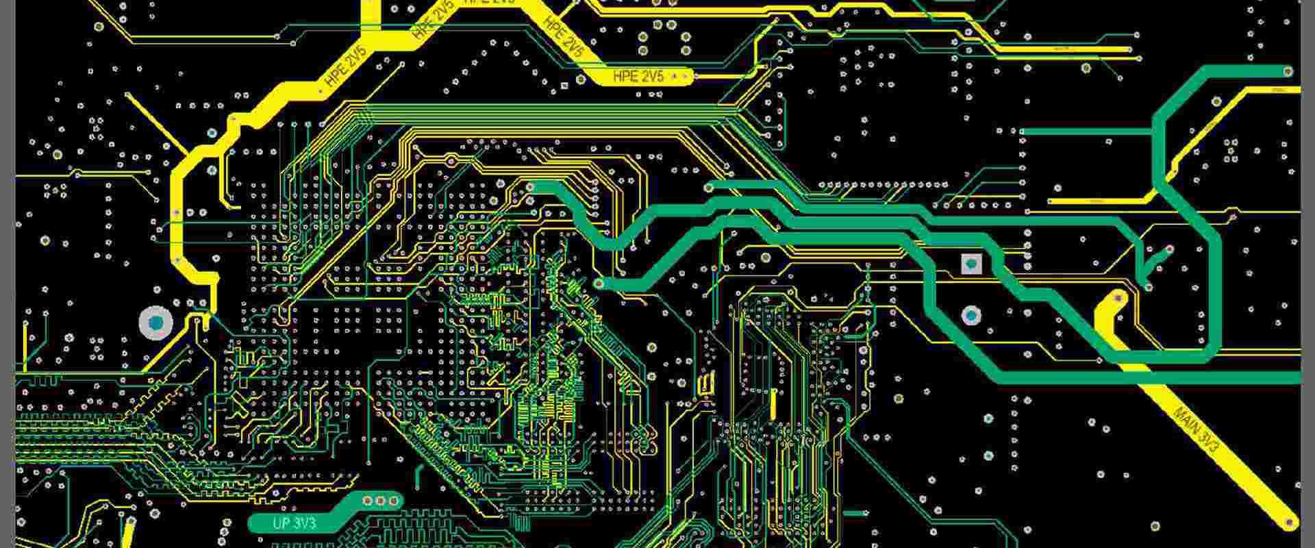
 Figure 12. Schematic Design
 Figure 13. Illustration of Routing
C4 Jinxiongdakejiyuan Huanguannan rd, Guanhushequ, Longhua district Shenzhen China
 sales@pcba360.com
 PCBA360
 +86-755-84717796
Certifications

Delivery


<

 Quote
Quote