
Automated optical inspection is a key technique used in the
manufacture and test of electronics board. AOI enables fast and
accurate inspection of PCB PCBA and in particular PCB to ensure that
the quality of product leaving the production line is high and the items
are built correctly and without manufacturing faults
For Bare printed circuit boards, The AOI test verifies the finished conductor trace image for deviations from the Gerber data and finds errors that the E-Test may not discover, such as (for example) narrowed, but still unbroken conductor traces.
The AOI test is especially important for the following application areas:
1. High frequency
2. High power loads
3. High data transmission rates
4. Op-amps with high amplification factors and input resistances
The inner layers of multilayer PCB use AOI to scan before they are pressed together. This guarantees the high reliability of multilayer boards.

The growth in the industrial sector is exponentially increasing to such an extent that we find too many suppliers and manufacturers in a particular sector say automobile sector. Similarly talking about electronic PCB manufacturing services, there are a large number of CEM (Contract Electronic Manufacturers) that provide services in this domain.
Some of them are simply the bare PCB manufacturers only, some of them are PCB Assemblers, some are turnkey solution providers i.e. they provide PCB mass manufacturing plus prototype PCB assembly both and also provide value added services in later stages after the PCB is fabricated and stuffed and finalized.
A very important in-process step while fabrication of PCBs is the inspection of PCB. This is inevitable in today’s complicated circuit design based PCBs where hundreds of components are stuffed upon the PCB to implement the inspection procedure. However there are commonly three types of inspection methods. Visual inspection, AOI and AXI (Automated X-ray Inspection). In this article we will discuss about AOI.
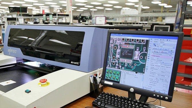
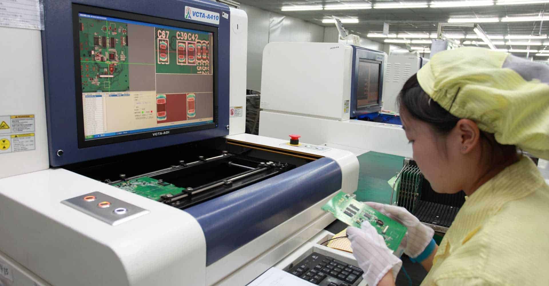
AOI as name implies is the automatic method of inspecting PCBs during fabrication process. The AOI setup usually contains the multiple high definition, high resolution and magnification cameras, with a strong light source, a core processing and memory unit and an operator.
Today as commonly the PCBs are starting from 4 layers hence the components are densely populated on board so it is extremely important that AOI is performed in different stages of PCB fabrication process. The AOI can be done of bare PCB as well as PCB assembled with electronic components.
AOI is important to ensure the quality of PCB according to standards, to identify the errors, faults and any anomaly in earlier stage so as to stop the process, rectify the fault and then let go the process again. This helps to reduce the too many faulty PCBs at the end of process . This ensures lesser counterfeit PCBs and so reduces overall pcb production cost. Unusually the AOI is carried out after the reflow soldering to find defects in solder joints early in the production line.
The AOI inspection is done by scanning the surface of the PCB board. The AOI machine fitted with HD color cameras that scans the surface with high magnification clearly showing on larger monitor screen the details of each section of PCB and each component of each section. The camera captures the image of the PCB surface through light source such as fluorescent or LED lights pcb or UV or infra red light.
The image is then compared with the pre-programmed data and fed in the memory of AOI processing system. The difference or Normalized Cross Correlation (NCC) if found greater than tolerance limit is displayed and indicated and process is stopped immediately. The higher the NCC the smaller the difference in captured and pre-programmed (template) images. The final decision to declare the board to be faulty and hence stop process depends on various algorithms running on AOI machine depending on pixel counts and NCC values.
The operator of AOI machine also visually checks the images captured by AOI machine on screen and hence can manually stop process as found necessary. The blob analysis is performed by separating the object image from background and then integrating or grouping the “blobs or pixels” of pixels based image and finding faults.
The AOI can be done before reflow to check for component placement, location and status i.e. defects not related to soldering. The post reflow AOI identifies defects in soldering joints, components and PCB board itself that may have caused due to thermal dynamics of reflow oven
The AOI machine can scan smallest components such as 01005, 0201 and 0402 package and IC packages like QFP, QFN, CSP and BGA and PoP only for surface inspection not for underneath the package inspection. It should be noted that components that are present under the body/package of IC cannot be inspected by AOI.
For this AXI is required. Because X-Ray can penetrate through the body then the grey scale images can be shown for the component identification beneath the IC package.
The AOI is an impressive method of automated inspection of PCBs on mass scale production line. The AOI can check for open and short circuits, wrong polarity of components, misplaced or missing components, wrong orientation of IC packages, stains, cuts, scratches, insufficient solder paste, solder bridges, cracked solder joints, excess solder, lifted leads, tombstoning, solder balls, billboarding, package height (3D AOI), coplanarity (3D AOI)
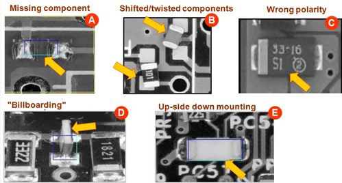
Wrong values of components, counterfeit component, BGA package shorts and opens, solder quality,
There are many reason as to why one should opt for AOI inspection rather than visual. But visual inspection is still incorporated in many PCB fabrication house. Some of the main reasons to select AOI over visual inspection are
1- Human eye can get tired and fatigue is common while doing visual inspection of tiny components on PCB. On the other hand machines do not get tired not fatigue
2- Human visual inspection is susceptible errors and can mistakenly miss the fault on PCB. While AOI machine will never miss a fault if that fault details are programmed in AOI machine memory. Hence accuracy of AOI is better than visual inspection
3- Humans can get sick of doing same type of job while machines can do the same job repeatedly, precisely forever.
4- AOI is helpful for mass production runs of PCB fabrication and assembly while visual inspection is not suitable for mass production and suitable for prototype level production
5- AOI is faster and can save time and money while visual inspection is slow and needs more focus and time to complete inspection
6- AOI is machine based inspection method hence it gives valuable data logging of types of errors or defect that occur in various stages of PCB fabrication and PCBA. While visual inspection many times do not record the faults and types of defect but can rectify the defects easily.
7- With AOI you will be assured that your PCB will be completely defect free and with visual inspection there are always chances that some defects are remaining
Summing up all we can say that AOI is utmost important aspect of PCB fabrication and PCB assembly processes. It is flexible to be implemented at any stage of process as per the requirements of user or needs. For mass production of complicated SMT based PCBs it is highly recommended to run AOI.
C4 Jinxiongdakejiyuan Huanguannan rd, Guanhushequ, Longhua district Shenzhen China
 sales@pcba360.com
 PCBA360
 +86-755-84717796
Certifications

Delivery


<
 Quote
Quote