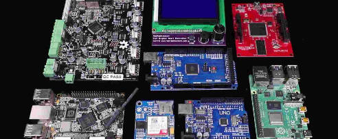
We all are familiar with Printed Circuit Boards (PCBs) to be the core of electronic products functionality. These PCBs are consisted of the hard green color board commonly seen in all electronic equipment when it is opened inside. These PCBs are fully loaded with electronic components like resistors, capacitors, ICs, inductors, transformers, chokes, jumpers and connectors and many other stuff. The components along with PCB copper tracks are connected with each other and designed to carry out one or more than one functions.
However it is utmost important that the PCB itself and the components residing on the PCB are not faulty and are not defected and connected correctly.
To check this, there are various tests that are performed by PCB manufactures or Contract Electronics Manufacturers (CEM) also called Electronic manufacturing Supplier (EMS). These tests are 1- In Circuit Test 2- Bed of Nails Test 3- Flying probe test. These tests are also called “Electrical Performance Test”.
These electrical test ensures that the bare PCBs or stuffed PCBs that leave the factory are comprehensively tested in the domain of electrical parameters. There are various types of electrical parameters like short circuit, open circuit, voltage, current, resistance and capacitance etc.
There are strength and weaknesses of each of the two electrical PCB testing methods for PCBs. ICT has its own advantages while FPT has its own, it depends upon the user requirement how the user want the PCB to be tested and what budget constraints of user are.

Actually the ICT testing requires a solid “fixture” that the CEM will develop to access the test point in the circuit / PCB. This fixture is different for every different PCB design and hence the CEM has to develop this fixture and it take a lot of time in development of fixture. But once the fixture is made it can be attached to the in-circuit test system to simply perform the ICT within few minutes. The fixture is the interface between the circuit tester and the PCB.
The ICT is also called the Bed of Nails test because the fixture is actually the nails or points that go directly in the circuit board. The in circuit tester is the matrix or array of sensors and drivers setup to perform measurement. The measurements like resistance, inductance and capacitance between two points in the PCB can be done using ICT. ICT can also detect open and shorts.
The ICT testing is suitable large run or mass production of a particular PCB. This is because the initial design and development cost of ICT fixture is very high and the design fixture is different for different PCB designs. The ICT testing can access most of the nodes of the PCB to test and measure but some nodes that are hidden/shielded or under a larger component so these nodes remain untested and hence confidence will be less that the board still have some faults located in nodes that remained unreached due to incapacity of nails/ICT fixture.

The flying probe test also called “Fixtureless Testing” on the other hand do not have a bed of nails fixture except it has a fixture to simply hold the bare or assembled PCB board. The PCB is moved on the conveyer belt and brought directly under the robotic architecture of flying mechanism of testing system. The flying probe test (FPT) is basically the system of automated robotic hands that can move in x, y coordinates to gain access to each and every point on entire PCB and use z axis to move the probe vertically towards and away from the PCB. The robotic arm end effector is actually the probe that is connected to the back end testing system. The testing system is pre-programmed to carry out different measurements like voltage, current measurement, and impedance measurement, components value like resistance, capacitance and inductance. The component orientation and component polarity detection is done by a high definition camera installed on the PCB flying probe setup. There are multiple probes (as few as 4 and as many as 20 needles) that can take measurement simultaneously of different parameters (voltage, current, resistance and continuity) between any two points on the PCB.
The PCB is fixed on the particular stand or fixture and the probes are “flying” at very high speed due to robotic arm both on top and bottom of PCB. The name flying is because the test probes are flying all the way on the PCB and can get access to any point on PCB as the FPT system is programmed.
The system is highly accurate the probes simply touch the test points on the PCB precisely and take measurements and then probes fly away from that point and take readings on other point of PCB. These probes are very sharp needle and interestingly do not damage the PCB while testing. With FPT, costs-per-unit are higher compared to ICT because of longer test cycle time periods per board (up to 15 minutes).

Both ICT and FPT have their pros and cons, it is up-to to the customer to decide which test methodology to select. These are 4 main factors that helps which method to select
Quality is a primary aim for any printed circuit board designer. Therefore a PCB fabricator needs to provide prior quality assurances when approached for assembly or fabrication services. A perfect quality assurance technique entails a PCB test process. It is therefore typical for most contract manufacturers to have varied testing methods. However, while varied, the industry always has universal testing standards.
Imagine the financial implication of getting your PCB design fabricated and having it fail immediately after it gets delivered. As an engineer or designer, it’s a chance you cannot risk. It becomes vital to have the fabricator conduct printed circuit board testing. The process comes as an integral part of the fabrication and assembly process. Consequently, plenty of dependable electronic manufacturers will provide a plethora of PCB testing techniques.
PCB testing happens at different levels. It happens at the bare printed circuit board level, the PCB raw materials level, and the printed circuit assembly product. Such tests ensure the proper functioning of the circuit as designed, and the materials used to withstand the intended application. As such, the PCB has to undergo testing to ensure qualification, conformance, and acceptance.
Testing and inspection often go hand-in-hand when it comes to circuit boards. It often covers a range of techniques that ensures the PCBs meet the set quality standards. The standards often determine the test, and with everything aimed at ensuring the proper functioning of the circuit board. Besides this, it also adherence to the project’s specifications and eradication any errors or defects.
Electric board tester for electrical testing and other PCB board testing approaches apply in these PCB tests and inspection processes. Remember, testing procedures aim to evaluate diverse components of printed circuit boards in-depth and ensure high standards. Additionally, tests focus on general PCB attributes, specific circuit board attributes, components, etc. So what does it all entail?
Printed circuit boards often have diverse and complex components that allow for their proper functioning. It entails components like capacitors, transistors, fuses, diodes, and resistors. During PCB development, the circuit board, complete with its components, undergoes a testing phase. Components that get tested include the following.
As much as each component comes in isolation, they often work complimentarily in a circuit board. However, monitoring and testing each component becomes vital to ensure optimum functionality of the PCB. But if you need testing or monitoring services, do not hesitate to contact us via our XDF PCB and Assembly website.
General testing of PCB aspects is important, and the same happens with its diverse components. However, all these often entail specific tests to ensure adherence to industry specifications. Some vital circuit board testing specifications entail MIL-PRF-31032, MIL-P-50884, MIL-PRF-55110, IPC-6018, IPC-6016, IPC-6013, and IPC-6012. Some of the specific tests to achieve these specifications include the following.
Other board material testing include the following
When submitting a PCB design, proper discussions with an electronic contract manufacturer should entail your preferred PCB testing methods. It should become a foundational factor under consideration when approaching an EMS. But it is impossible to have a fruitful discussion without understanding the diverse types of testing methods involved in PCB fabrication and mass production. This section will canvass the primary testing method in depth and their importance in the PCB production process.
It represents a robust PCB testing approach. In-circuit testing often proves costly, though this also depends on the fixture and board size, among other aspects. The ICT test, alternatively inferred as a bed-of-nails test, actuates and powers the specific circuitry on the circuit board. It often entails 100% coverage by design, though it covers about 85-90% coverage in most instances. However, the coverage, albeit not 100%, often comes devoid of any human error.
In-circuit testing deploys fixed probes that get laid out a particular way and which matches the PCB design. It is the probes that check for the solder connection integrity. The ICT tester pushes the circuit board to the bed containing the probes to initiate the test. Predesigned access points exist on the board, allowing the testing probes to connect with the circuit. Consequently, the pressure applied to the connection ensures it all stays intact.
In-circuit testing often gets performed on BGAs (ball grid arrays) or bigger connections. It applies to “mature” products with very little revisions anticipated. However, a lack of DFM (design-for-manufacturing as an objective in your PCB production may make in-circuit testing impossible to carry out. Unfortunately, it is impossible to switch mid-way into an in-circuit approach.
Benefits
The PCB flying probe test is a valuable and less expensive testing option compared to in-circuit testing. It is not powered responsible for checking for shorts, opens, capacitance, diode issues, and resistance. It uses needles attached to the PCB probe on the x-y grid from the basic CAD. However, the ECM program must coordinate and matches the circuit board before running the program.
The flying probe test PCB process is essential in printed circuit board assembly for production and prototype volume testing. It arises from the increasing need for innovative PCB features such as increased board access, test speeds, repeatability, and reliability.
Since it uses PCB test probes that fly, it requires no custom fixtures. However, it is important to note that originally, the design permitted the testing of bare boards. It has since evolved into a go-to, all-encompassing test, ideal for PCB assembly.
Benefits
It is a unique testing approach that uses a 2D or 3D camera in taking pictures of the printed circuit board. The images get relayed into a specific program that compares the board images with a comprehensive schematic. Any board that fails to match the reference schematic at a certain cut-off point gets flagged for inspection.
Automated optical inspection becomes useful in detecting issues promptly and preventing any immediate shut down of the production process. However, the testing approach cannot power up the board and may fail to cover 100% of every part type. Additionally, it is advisable to always rely on other testing approaches besides the AOI. Some of the ideal combinations include the following.
Benefits
It comes with an extra intense testing type for printed circuit boards. By design, it detects any early failures and develops a load capacity. The intensity by which it works can destroy the parts getting tested.
Burn-in testing works by pushing power at its maximum and within the specified capacity through the electronic device. It happens for about 48-168 hours where power gets run through continuous. Whenever a board fails this test, it gets referred to as infant mortality. On this basis, the quota fails to determine the suitability of the PCB’s quality for deployment, especially medical and military applications.
However, burn-in testing is not ideal for every PCB project, as it makes sense for some projects. It can help prevent embarrassing product launches or dangerous products from reaching customers. Burn-in testing has the capability of shortening the lifespan of a product, especially when it subjects your board to undue stress than it can handle. Therefore, you can reduce the test limit to shorter periods to avert overstressing the PCB whenever you cannot identify defects.
Benefits
Popularly inferred to an AXI, the testing approach proves more of an inspection instrument for many electronic contract manufacturers. It entails a testing method where the X-ray technician identifies defects by looking at solder connections, barrels, and internal traces.
X-ray inspection can come either as a 2D or 3D AXI test. The 3D testing provides a quicker testing timeline. The testing process proves capable of checking elements that are not apparent to the naked eye. It can include BGA (ball grid array) packages complete with solder joints and connections. While a useful test, it requires an experienced and trained operator to carry out.
It is also prudent to remember that your electronic contract manufacturer will not necessarily inspect each board layer using the x-ray machine. Yes, you can see through to pinpoint internal defects. However, it is a tedious, expensive, and time-consuming process for ECMs and the client.
Benefits
Most electronic contract manufacturers perform a functional test for verification purposes that the electronic product will power up. It arises since most customers love this old-fashioned testing approach. The test requires external equipment pieces, fixtures, and requirements like MSHA, UL, and other quality standards.
A functional test’s parameters often get specified by the PCB consumer. However, some electronic contract manufacturers can assist with the development and designing of such tests. It also takes time and may not prove ideal if you need to quickly get your PCB product to the market. However, it can come in handy in saving face and money from a longevity and quality standpoint.
Benefits
Other functional test types can apply when checking a printed circuit board project based on the prevailing circumstances. The functional test can vary since a functional test aims to test and verify the PCB’s behavior when deployed. Aspects such as the PCB’s development besides procedures vary from one type to the other.
Other functional tests that apply based on the PCB variations include the following,
Benefits
While testing always proves an essential piece of the PCB development process, it is possible to ensure quality without over-reliance on testing. A key way of ensuring this entails the adoption of the best design techniques. Such techniques help in protecting your printed circuit board besides helping it pass tests and inspection. It includes design for manufacturing, design for test, design for assembly, and design for the supply chain.
In most instances, PCB designers deploy such techniques in the simulation and schematics stage. Ensuring the printed circuit board meets the various standards and parameters is vital before it gets sent into manufacturing.
It involves arranging the printed circuit board typology to align with the fabrication or manufacturing process. Because of this, the layout typology aims to mitigate challenges that happen during the assembly and fabrication process. DFM problems include the following.
It helps by making the assembly process easier, especially for complex PCB designs. Here, minimizing the material inputs, pick easy-to-get components, and provide adequate space between components. Additionally, application of the general design standards and make clear and accurate marks for components. It is crucial to implement the DFA early during the design of the project. Printed circuit board testing programs are also available to assist with DFA standard conformation during the design process.
It helps in making the testing more comprehensive besides reducing the testing costs. PCBs with DFT considered in their design makes it simpler to locate and detect failures. Therefore, it makes it simpler to run checks and test accurately and quickly.
Often unconsidered by many designers, DFSC is crucial in ensuring a fair match-up of components with the anticipated PCB lifecycle. If not considered, a component may become obsolete in the life cycle of the PCB. Replacing such components may prove difficult and more expensive. Therefore, whenever you consider DFSC early will ensure a longer product’s lifespan besides saving you money.
Circuit board designers need to consider all the PCB test methods responsible for guaranteeing the quality of PCBs. It helps reduce the cost of production as a result of product failures and helps increase the product lifecycle of PCBs. Therefore, before engaging your electronic contract manufacturer, consider the insight on the diverse aspects contained in the article. It will smoothen the discussions with your ECM and set expectations upfront.
C4 Jinxiongdakejiyuan Huanguannan rd, Guanhushequ, Longhua district Shenzhen China
 sales@pcba360.com
 PCBA360
 +86-755-84717796
Certifications

Delivery


<

 Quote
Quote