PCB reverse engineering
PCB reverse engineering (also known as reverse technology) is a process of printed circuit board design technology reproduction, reverse analysis and research of a target PCB board. It is also to deduce and obtain the design of the product’s processing flow, structure, functional characteristics, and technical specification elements to produce products with similar, but not exactly the same, functions. Reverse engineering originates from hardware analysis in the commercial and military fields. Its primary purpose is to directly analyze the finished product and push out its design principle when the necessary production information cannot be easily obtained.
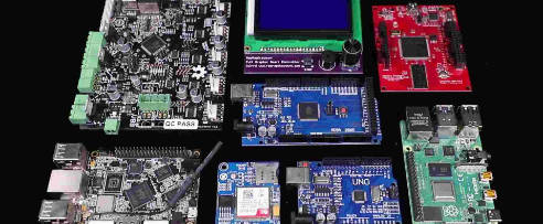
Another service we offer at XDF is Printed Circuit Board Reverse Engineering. We can take your sample, including components, and completely reverse engineer it. We create all the data you need to make duplicates. We can even reverse engineer boards that include programmed IC‘s, custom parts, and obsolete parts.
To begin, we identify every electronic component on the board. We then create a rough bill of material for the project. Every part of the board is carefully photographed. A photocopy of the board is blown up and mounted. Each component is removed and glued to its location on the photocopy. The bill of material is refined as values are measured for resistors and capacitors. When the bill of material is completed, parts are then procured, and the board is scanned on a calibrated scanner to recreate the trace pattern. Finally, the new bare boards are created. An assembled sample is sent to the customer to ensure proper function prior to project completion. This becomes a ‘golden board’ from which all others are duplicated.

It is the process of disassembling and analyzing a physical product to generate documentation, remanufacture, and determine how it was designed and operates. Often the documentation even allows a customer to improve their product to surpass competitors.
XDF is the number one for electronic reverse engineering in Shenzhen, China. With over ten years of engineering experience specializing in reverse engineering of electronic hardware, our team is up to any job. We can help you by reverse engineering, remanufacturing obsolete and unsupported electronic circuit boards and card assemblies. Electronic hardware reverse engineering is the process of determining in our laboratory how an item was designed and how it operates in order to reproduce it from the printed circuit board to the schematic. We can not only repair your PCB, but we can copy or clone your printed circuit board (assuming it is no longer supported by the OEM, PCB to schematic and ensuring the legality of reverse-engineering the product) or even upgrade your hardware, it making sure that the replacement unit is a replica in form, fit and function. Before we start work, we investigate and evaluate the product to ensure that no intellectual property rights are breached. XDF is committed to providing the best customer support in the PCB clone and PCB copy industry, and we want you to use XDF when you think about reverse engineering a PCB.
PCB Reverse engineering can use 3D scanner technologies such as laser scanners, structured light source converters, or X-ray tomography to measure dimensions based on existing physical components, and then construct 3D virtual models through CAD, CAM, CAE, or other software.
that is, on the premise that there are already physical, electronic products and circuit boards, the reverse research and development technology
The more popular reverse engineering technology is PCB copy board and chip decryption. PCB reverse design or PCB reverse research and development analyzes the physical electronic products and circuit boards, reverse engineer the original product PCB files, bill of materials (BOM) files, schematic and technical files, and PCB silkscreen production files. These technical and production files are used for PCB board manufacturing, component soldering, flying probe test, circuit board debugging, and complete the full copy of the original circuit board template. Chip decryption, also known as IC decryption or MCU decryption, directly obtains the encrypted programming file in the MCU through specific equipment and methods. You can then copy and program the chip yourself or disassemble it for your reference and research. With the help of special equipment or self-made equipment, a single-chip attacker uses vulnerabilities or software defects in the single-chip chip design to extract critical information from the chip and obtain the program in the single-chip microcomputer through a variety of technical methods.

Copy board is also called cloning or imitation, which is the reverse technology research of the designed PCB board. In a narrow sense, the copy board only refers to the extraction and restoration of PCB files of electronic product circuit boards and the use of files for circuit boards. The process of cloning; in a broad sense, copying the board not only includes the technical process of extracting circuit board files, circuit board cloning, and circuit board imitation but also includes modifying circuit board files (e.g., changing the board) and performing electronic product shape molds. Three-dimensional data extraction and model imitation (e.g., copying) imitates electronic components on electronic product circuit boards, decrypts encrypted chips or single-chip computers on circuit boards, and disassembles the electronic product system software—all the technical processes of a full set of cloning of electronic products.
Get a PCB. First, record the model, parameters, and position of all components on the paper, especially the direction of the diode, the triode, and the direction of the IC gap. It is best to use a digital camera to take two photos of the location of the components. Since PCB circuit boards are getting more advanced, some of the diode transistors above are not easily noticeable.

Remove all components and remove the tin in the PAD hole. Clean the PCB with alcohol and put it into the scanner. When scanning occurs, you need to raise the scanned pixels slightly to get a clearer image. Then lightly polish the top and bottom layers with water gauze paper until the copper film is shiny, put them in the scanner, start PHOTOSHOP, and scan the two layers separately in color. Note that the PCB must be placed horizontally and vertically in the scanner; otherwise, the scanned image cannot be used.
Adjust the contrast and brightness of the canvas until the parts with and without copper film have strong contrast. Then turn the second image into black and white, and check whether the lines are clear. If not, repeat the process. If it is clear, save the picture as black and white BMP format files TOP.BMP and BOT.BMP. If you find any problems with the graphics, you can also use PHOTOSHOP to repair and correct them.
Is to convert the two BMP format files into PROTEL format files and transfer two layers in PROTEL. For example, the positions of PAD and VIA so that the two layers coincide. That will indicate that the previous steps are well done. If there is a deviation, repeat the third step. Therefore, PCB copying is a task that requires patience because a small problem will affect the quality and the degree of matching after copying.
Is to convert the BMP of the TOP layer to TOP.PCB. Pay attention to the conversion to the SILK layer, which is the yellow layer. Then you can trace the line on the TOP layer and place the device according to the drawing in the second step. Delete the SILK layer after drawing. Repeat until all the layers are drawn.
Is to import the TOP.PCB and BOT.PCB in PROTEL. It is okay to combine them into one picture.
In the seventh step, use a laser printer to print the TOP LAYER and BOTTOM LAYER on transparent film (1:1 ratio), put the film on that PCB, and compare whether there are errors. If they are correct, you are done.
A reverse board that is the same as the original board was born, but this is only half the work. It is also necessary to test whether the electronic technical performance of the copy board is the same as the original board. If it is the same, it is complete.
Remarks: If it is a multi-layer board, you need to carefully polish to the inner layer and repeat the copying steps from the third to the fifth step. Of course, the naming of the graphics is also different. It depends on the number of layers. Generally, double-sided copying requires much more straightforward than the multi-layer board. The multi-layer copy board is prone to misalignment, so the multi-layer board copy board must be cautious and careful (the internal vias and non-vias are prone to problems).

Get a good circuit board to see if there are any components with a high position. If so, make a detailed record of the component location number, component package, temperature value, etc. You must scan it as a backup before disassembling the components. After removing the higher components, SMD and some smaller components are left. At this time, perform a second scan and record the image. It is recommended that the resolution be 600dpi. Be sure to remove the dirt on the PCB surface before scanning to ensure that the IC model and the characters on the PCB are clearly visible in the picture after scanning.
Use a small air gun to heat the component to be removed, clamp it with tweezers, and let the pipe wind blow it away. Remove the resistor first, then the capacitor, and finally the IC. And record whether any components have been dropped and installed reversely. Before disassembling, prepare a table with the number, package, model, value, and other record items. Then paste double-sided tape on the column of the component record. After the write position number, paste the removed components one by one to the corresponding position of the position number. Then use the bridge to measure the value of all the components. Some components will change under high temperature, so they should be measured after the device temperature decreases, giving a more accurate measurement. After the measurement is completed, the data is input to the computer for the archive.
Using flux, remove the remaining tin dross from the PCB surface where the components were removed with a tin suction wire. Adjust the temperature of the soldering iron appropriately according to the number of layers of the PCB. Since the multi-layer board heats up quickly and is not easy to melt the tin, increase the soldering iron’s temperature, but not too high to avoid burning the ink. Wash the board from which the tin has been removed with board washing water or thinner water and then dry it.
After scanning the surface image, set them as the top and bottom layers respectively, and convert them into bottom images that can be recognized by various copying software. According to the bottom images, first package the components, including small silkscreen, pad aperture, positioning holes, etc. After all the components are completed, put them in the corresponding position, adjust the characters to make the font, font size, and position consistent with the original board. Then proceed to the next step.
Use sandpaper to sand off the silkscreen, ink, and characters on the PCB surface to expose bright copper (there is an important trick to sand the pad. The sanding direction must be perpendicular to the scanning direction of the scanner). Of course, there is another way to heat the ink with alkaline liquid, but it takes a longer time. Usually, the former method is more environmentally friendly and harmless to the human body. Having a clear and complete PCB bottom map is an essential prerequisite for copying a good PCB board.
For a multi-layer PCB, the order of copying boards is from outside to inside. Take an 8-layer board as an example:
First, remove the first and eighth layers of ink, copy the first and eighth layers, and polish off the first and eighth layers of copper. Afterward, copy the second and seventh layers, then the third and sixth layers, and finally, copy the fourth and fifth layers. During the operation, pay attention to the error between the scanned image and the real board, and it should be handled appropriately to make its size and direction consistent with the real board. After ensuring that the size of the base map is correct, start to adjust the position of the PCB components one by one to make them coincide entirely with the base map for the next step to place vias, trace wires, and lay copper. In this process, attention should be paid to details such as the width of the board, the size of the aperture, and the parameters of exposed copper.
A perfect inspection method will directly affect the quality of a PCB drawing. Using image processing software, combined with PCB drawing software and the physical connection of the circuit can make a 100% accurate judgment. Impedance has a considerable influence on the high-frequency board. In the case of only the physical PCB, you can use an impedance tester to test or slice the PCB, measure the copper thickness and layer spacing with a metallurgical microscope. Analyze the dielectric of the substrate constant (usually FR4, PTFE, RCC as the medium) to fully ensure that the PCB indicators are consistent with the original board.
Precision adjustment correction
The accuracy of the copy board depends on two links: the accuracy of the software and the accuracy of the original image. All kinds of copying companies have different technical capabilities in copying accuracy. Some companies have inferior copying technology and low copying accuracy, while some have robust copying technology, and the copying accuracy can reach less than 1mil.
For software accuracy, using 32-bit floating-point representation can say that there is no accuracy limit, so the most important thing depends on the image accuracy of the original scan. For example, if you use 1 million pixels to take a photo, it clear in a five-inch photo. But if you want to develop it into a 20-inch photo, it will not clear at all. The reason is the same for circuit boards with high precision requirements. If you want to copy a very high-precision PCB diagram, choose a higher DPI when scanning.
The meaning of DPI is how many dots per inch. That is to say, the distance between every two points on the scanned image is 1000/DPI, the unit is mil.
If the DPI is 400, then the distance between two points on the image is 1000/400 = 2.5 mil, which means that the accuracy at this time is 2.5 mil.
This is the most scientific basis, so some people say that accuracy can reach 1mil or less; that is a premise. The accuracy of the copy board mainly depends on the original scanning accuracy.
In summary, when scanning the board, setting the DPI should be based on the accuracy required by the actual board. If the cell phone board sub-line spacing accuracy is required to be less than 1mil, then the scan DPI should be set above 1000DPI. Scanners on the market can meet this condition.
The higher the DPI, the clearer the picture and the higher the accuracy, but the disadvantage is that the picture is too large and requires higher hardware requirements, so it should be set according to the specific situation. For boards with general precision, 400DPI is generally good, and mobile phone boards can be set above 1000DPI.

The quality of the copying software mainly depends on its functionalities. It is best to do all the work in the copying software, as the efficiency will be high. If component placement support PROTEL99SE, that would be ideal. 99SE component library is plentiful and can be downloaded on the Internet. This is also a very critical matter. The era of hand-made components for copying boards has passed because many components such as BGP have hundreds of components, and it is too expensive to build components manually.
For the stability and reliability of the circuit, it is generally necessary to connect a large piece of copper to the power supply or ground when designing the circuit to reduce the noise and interference of the circuit. Therefore, it is related to the problem of copper paving on the network. For complex circuit boards, many of the copper pavings are to be connected, and many are to be isolated. If this problem is not resolved, copper paving cannot be achieved. Here must define the network to lay copper (“the same network is connected, but different networks are isolated”). Simply filling everything with copper will cause a short circuit. This is also a vital issue for measuring copy board software.
After choosing the software with desirable functionalities for the copying of double-layer and multi-layer boards, technical experience and skills need to be applied. The same double-layer or multi-layer PCB board has holes in the same position, but the circuit connection is different. When drawing the wiring rules of the original board in the copying software, stack the top-level PCB file that has been copied from the double-layer board. On the scanned image of the other layer, the vias of the two overlapped, then set the top line and silkscreen not to display, and trace the lines of the other layer according to the position of the vias. In this way, the exported PCB file contains both sides of the double panel. data.
The same applies to multi-layer boards, except that the surface layer needs to be polished with sandpaper after drawing the surface PCB file map to expose the internal wiring rules, and then copy it out with the same technique with the help of copying software.
The most commonly used copy board software on the market is PROTEL99SE, and the other is quickpcb 2005 V3.0 and various versions of the color copy board software.
Protel99SE was initially used as a 32-bit EDA design software under the Windows9X/2000/NT operating system. It adopts a design library management mode and can be designed for networking. It has robust data exchange capabilities and openness, and 3D simulation functions. The design software can complete circuit schematic design, printed circuit board design, and programmable logic device design, and can design 32 signal layers, 16 power-ground layers, and 16 machined layers.
All operations of quickpcb 2005 V3.0 software conform to most designers’ operating habits, which can significantly improve the efficiency of board copying and relieve the operators of detection pain. The one-time pass rate of the copy board can also be further guaranteed.
Features:
Place pads, holes, lines, arcs, vias, components, FILL, POLYGON, text.
Attribute setting of each element, grid setting.
CTRL key automatically captures the grid and element center.
SHIFT key to select, go to select, cut, copy, delete, rotate, mirror, and repeat functions.
32-layer setting function, zoom display.

Which industry and product types are involved in PCB reverse engineering? There is no unified answer to the types of electronic products that can be copied because each PCB reverse engineering company has different technical strengths. The field and type are also different. However, in general, with the improvement of the copy board industry’s overall technical capabilities, the copy board’s scope and the fields involved are continually expanding. Large copy board companies such as the orange box can already clone any electronic products. For detailed copy board types and technical implementations, you can contact XDF for consultation. From the industry perspective, the typical types of electronic products that can be copied are mainly:
High-frequency signal generator, power signal generator, low-frequency signal generator, high-frequency signal generator, high-precision instrument copy board, digital pulse frequency measuring instrument, analog frequency measuring instrument, counter, counter spread spectrum device, time measuring instrument, Special counters, frequency standards, frequency calibration phase comparators, network characteristic testers, network analysis radar comprehensive testers, microwave power amplifiers, microwave instruments, microwave attenuators, microwave filters, communication measuring instruments, etc.
PHS PCB copy board, GSM mobile phone, CDMA mobile phone, wireless module, GPS locator, cable TV set-top box, terrestrial broadcast set-top box, satellite broadcast set-top box, etc.
Server motherboard, switch motherboard, wireless router, eight-way video card, VPN equipment, wireless network card, Internet phone, VOIP gateway, high-end computer motherboard card, high-end network router fiber network switch motherboard, wireless base station, terminal product motherboard, SDHPCB copy board, DWDMPCB copy board, LAN SWITCH, ADSLPCB, high-end computing equipment, optical fiberboard, network routing copy board, driver motherboard copy board, terminal products, network hard disk copy board, network camera, etc.
MP4 PCB copy board, digital learning machine, mobile hard disk box, multimedia hard disk player, portable DVD, game peripheral PCB copy board, multimedia electronic equipment PCB copy board, home theater, car DVD, TVPCB, car control board, USB copy board, digital camera PCB copy board
Security monitoring equipment, industrial control mainboard, mainboard, UPS, industrial power supply industrial control board PCB copy board, rust machine control board, image monitor, cutting control board, SMT industrial control board, machine tool control board, inverter, industrial control switching power supply, Boiler industrial conductivity controller, industrial control single-chip microcomputer, electromagnetic heating control cabinet, general engraving machine.
Military Projects: fire control board, radar, etc.
Case:

If there is a four-layer board, the components have been removed, and the surface is clean, to copy it into a PCB file, proceed as follows:
⒈ Scan the top board, save the picture, and name it top.jpg. At this time, the scan DPI can be set according to the density if the setting is 400DPI.
⒉ Scan the bottom board, save the picture and name it bottom.jpg.
⒊ Grind out the middle layer 1 with coarse sandpaper, leak out the copper skin, scan the picture after cleaning it, and name it mid1.jpg.
⒋ Grind out the middle layer 2 with coarse sandpaper, leak out the copper skin, scan the picture after cleaning it, and name it mid2.jpg.
⒌ Adjust each picture horizontally in PHOTOSHOP (select the picture and ensure that the picture is level, so that the line that goes out is refined, and multiple pictures are easy to align up and down). It is recommended to mirror the bottom image horizontally so that the top and bottom images are in the same direction. The upper and lower positioning holes are also the same. Finally, save each picture as a BMP file, such as: top.bmp, bottom.bmp, mid1.bmp, mid2.bmp. Note here that you don’t need to crop the picture exactly. It’s better to leave some margin; adjust the picture level, and you’re done.
⒍ Open the color copy board software, from the main menu “File” -> “Open BMP file,” select top.bmp file to open.
⒎ After setting the DPI, you can copy the top-level map, first select the layer to the top-level, and then start to put components, vias, wires, etc.
⒏ After putting everything at the top level, save the temporary file (both in the manual and help, you can select it through the menu or the button on the toolbar), and name it top-1.dpb (the name saved at different times in the middle). It is recommended to give names with different numbers, such as top-1.dpb, top-2.dpb, to avoid the damage of the last file due to computer failure, but the previous version of the file can be restored and reduce the loss. This is a suggestion, see personal preference Up).
⒐ Close the current picture window (note that only one picture can be opened at a time, never open multiple pictures).
⒑ From the main menu “File” -> “Open BMP File,” select the bottom image bottom.bmp, and then open the temporary file top-1.dpb. At this time, you will find that the top-level drawing is not aligned with the bottom background image. Press Ctrl-A combination of keys, select all the placed primitives, press the up, down, left, right cursor keys or 2, 4, 6, 8 number keys on the keyboard to move as a whole. Select several reference points and the corresponding point pairs of the background image. When it is accurate, you can choose the current layer as the bottom layer at this time, and open the bottom layer line, pad, fill, etc. What if the line on the top layer blocks the bottom layer? It’s very simple. You can select “Layer Color Settings” from the “Options” in the main menu and click off the top layer. The top silkscreen can also be turned off. After copying the bottom layer, save the temporary file as bottom-1.dpb, or save the PCB file as bottom-1.pcb, at this time, the file of the same and combined layers.
⒒ The copying process of the same middle layer is the same. Repeat steps 9 to 10, and the final output PCB file is the PCB diagram of the four layers combined and exactly the same as the actual product.
C4 Jinxiongdakejiyuan Huanguannan rd, Guanhushequ, Longhua district Shenzhen China
 sales@pcba360.com
 PCBA360
 +86-755-84717796
Certifications

Delivery


<

 Quote
Quote